Showing posts with label converter. Show all posts

Tuesday, November 18, 2014

DC DC Converter 12V to 24V

This simple circuit is a DC-DC converter that converting up 12V source to a 24V. It can be used to run radios, small lights, relays, horns and other 24V accessories from a 12V vehicle with a maximum draw of about 800mA.


This DC-DC Converter can be used to charge one 12V battery from another, or step up the voltage just enough to provide necessary overhead for a 12V linear regulator. Using one op-amp as a squarewave oscillator to ring an inductor and another op-amp in a feedback loop, it wont drift around under varying loads, providing a stable 24V source for many applications. With a wide adjustment in output this circuit has many uses. 

Parts List
R1-R4,R7-R8 100K 1/4W Resistor 
R5 470 Ohm 1/2W Resistor 
R6 10K Linear Pot 
C1 0.01uF Mylar Capacitor 
C2 0.1uF Ceramic Disc Capacitor 
C3 470uF 63V Electrolytic Capacitor 
D1 1N4004 Rectifier Diode 
D2 BY229-400 Fast Recovery Diode See Notes
Q1 BC337 NPN Power Transistor 
U1 LM358 Dual Op Amp IC 
L1 See Notes 
MISC Board, Wire, Socket For U1, Case, Knob For R6, Heatsink for Q1

DC- DC Converter Notes 
1. R6 sets the output voltage. This can be calculated by Vout = 12 x (R8/(R8+R7)) x (R6B/R6A). 
2. L1 is made by winding 60 turns of 0.63MM magnet wire on a toroidial core measuring 15MM (OD) by 8MM (ID) by 6MM (H). 
3. D2 can be any fast recovery diode rated at greater then 100V at 5A. It is very important that the diode be fast recovery and not a standard rectifier.4. Q1 will need a heatsink.
Read More..

Monday, November 17, 2014

12V to 20V DC converter

DC To DC Converter circuit used to be an alter tegngan voltage DC to DC with different concepts. DC to DC converter circuit +12 V to + /-20V is working to change the battery voltage from 12V DC to 20V DC voltage symmetrical. DC to DC converter circuit is often applied to the power amplifier udio on car audio systems. DC to DC converter circuit uses a TL494 IC as power plsa for the converter. TL494 IC is a PWM controller with an adjustable frequency from 40-60Hz through a potentiometer. Then from the TL494 PWM signal is given to the driver MOSFET inverter TPS2811P to be given to the power inverter with 2 units of MOSFET transistors. Circuit details can be seen in the figure following the DC to DC converter.

DC To DC converter circuit +12 V To + / - 20V

+12V

List Components DC To DC Converter +12 V To + / - 20V
R1, R2 = 10
R3, R4, R6, R7 = 1k
R5 = 22k
R8 = 4.7k
R9 = 100k
C1, C2 = 10000uF
C3, C6 = 47 u
C4 = 10U
C5, C7, C14 = 100n
C8, C9 = 4700u
C12 = 1N
C13 = 2.2u
U1 = TL494
U2 = TPS2811P
Q1, Q2 = FDB045AN
D1-D4 = 1N5822
D5 = 1N4148
FU1 = 10A
L1 = 10U
L2 = ferrite BEAD
RV1 = 2.2k
RV2 = 24k
T1 = TRAN-3P3S
DC To DC converter circuit +12 V To + / - 20V is capable of supplying up to 100W and can power supplying currents up to 3A. In making DC To DC Converter +12 V To + / - 20V has to be careful and cautious because there are parts of DC To DC Converter +12 V To + / - 20V in the form of an AC circuit.
Read More..

Saturday, October 25, 2014

455kHz IF Receivers DRM Down Converter

This project came about due to my interest in a new form of radio transmission called DRM, which stands for "Digital Radio Mondiale" (see www.drm.org). This is a new form of digital shortwave transmission. A few devices are available from Europe for decoding the digital signals but are expensive. I decided instead to modify an existing circuit, using a stable purpose-built 470kHz ceramic resonator as the oscillator, rather than the original unstable L/C version. The 455kHz IF signal from a shortwave receiver is fed into the input (pin 1) of a double-balanced mixer and oscillator (IC1) via a level adjustment pot (VR1). The NE506’s output (pin 4) is then AC-coupled to a PC’s sound card input for processing. With the capacitor between pins 5 & 7 set to 150pF, the oscillator frequency should be around 467.5kHz. You can check if the oscillator is working by putting it near a receiver tuned to 467kHz. You should hear a beat frequency.

Circuit diagram:DRM
DRM DownConverter Circuit Diagram For 455kHz IF Receivers

The IF signal of 455kHz is mixed with 467kHz, giving an output with a centre frequency of 12kHz. Sound cards should have no trouble sampling the 10kHz-wide DRM signal. A number of software-defined radio applications were found to work well with this converter. These applications perform all of the demodulation (SSB, AM, FM, etc) and various other DSP functions. If all is well, connect your 455kHz IF to the input and your computer sound card to the output. Run the Dream software (see http://drm.sourceforge.net), and tune to 6095Khz (RNZI), or 1440Khz (SBS). You should see the Dream software lock onto the DRM transmission and audio should start playing from the computer speakers. The NE602AN mixer/oscillator and 470kHz resonator are available for a cost of $12.50 - email the author for more details at jwtitmus@bigpond.com. A CD with various software defined receivers as well as the latest Dream software decoder is also available.
Author: John Titmuss
Copyright: Silicon Chip Electronics
Read More..

Wednesday, October 15, 2014

Simple Frequency Voltage Converter Circuit Diagram

This is the simple frequency voltage converter circuit diagram. Teledyne Semiconductor`s Type TSC9402 is a versatile IC. Not only can it convert voltage into frequency, but also frequency into voltage. It is thus eminently suitable for use in an add-on unit for measuring frequencies with a multimeter. 

Only a few additional components are required for this.. Just one calibration point sets the center of the measuring range (or of that part of the range that is used most frequently). The frequency-proportional direct voltage at the output (pin 12—amp out) contains interference pulses at levels up to 0.7 V. If these have an adverse effect on the multimeter, they can be suppressed with the aid of a simple RC network. 

The output voltage, U0, is calculated by: tfo=C/rei(Ci + 12 pF) R2fm Because the internal capacitance often has a greater value than the 12 pF taken here, the formula does not yield an absolute value. The circuit has a frequency range of dc to 10 kHz. At 10 kHz, the formula gives a value of 3.4 V. The circuit draws a current of not more than 1 mA.

Frequency Voltage Converter Circuit Diagram

Read More..

Wednesday, August 27, 2014

Build a Power Saving Intermittent Converter Wiring diagram Schematic

Build a Power Saving Intermittent Converter Circuit Diagram. This Power-Saving Intermittent Converter Circuit Diagram switches its dc/dc converter, IC1, off whenever the large filter capacitor, C6, has sufficient charge to power the load. This particular schema uses a dc/dc converter that produces 115 Vdc from, a 9-Vdc input; you can tailor the schema to suit other converters. The heart of the schema is a 555 timer configured as a dual-limit comparator. Thus, the 555 turns the converter on or off, depending on the voltage across C6. 

The 555`s complementary output lights the charge LED when the FET is on. Initially, the voltage on C6 is zero, and the 555`s output turns on the FET, Ql, in turn, enabling the converter to run, which charges C6. When the voltage on the capacitor reaches the value set by R3, the 555 turns the converter off. Then, C6 slowly discharges into the combined load of the voltage divider (R2, R3, and R4) and the reverse-biased blocking diode, Dl. When the voltage falls below 1/3 Vcc, the 555 restarts the dc/dc converter. 

If this schema powers a load that periodically goes into a zero-power, shutdown mode, the 555 switches the dc/dc converter on full time whenever the load kicks in. When the supply voltage falls below 7.5 V, the output of the converter is no longer high enough to charge, the LED doesn`t light. The schema uses 205 mA when the converter is on and 10 mA when the converter is off. The duty cycle comprises a 5-s on period, a 150-s off period, and it represents a 92% power reduction. You can further reduce power consumption by removing the charge LED and using a CMOS 555 and a CMOS 78L05 regulator.

Power-Saving Intermittent Converter Circuit Diagram

Power-Saving


Power-Saving Intermittent Converter Circuit Diagram
Read More..

Friday, August 22, 2014

9V to 3V converter


This schema can generate 3V from 9V power supply.Here I have used common Famous IC LT1073.


Read More..

Thursday, August 21, 2014

Build a Converter VGA to BNC Adapter

There are monitors which only have three BNC inputs and which use composite synchronization (‘sync on green’). This schema has been designed with these types of monitor in mind. As can be seen, the schema has been kept very simple, but it still gives a reasonable performance. The principle of operation is very straightforward. The RGB signals from the VGA connector are fed to three BNC connectors via AC-coupling capacitors. These have been added to stop any direct current from entering the VGA card. A pull-up resistor on the green output provides a DC offset, while a transistor (a BS170 MOSFET) can switch this output to ground. It is possible to get synchronisation problems when the display is extremely bright, with a maximum green component.

In this case the value of R2 should be reduced a little, but this has the side effect that the brightness noticeably decreases and the load on the graphics card increases. To keep the colour balance the same, the resistors for the other two colors (R1 en R3) have to be changed to the same value as R2. An EXOR gate from IC1 (74HC86) combines the separate V-sync and H-sync signals into a composite sync signal. Since the sync in DOS-modes is often inverted compared to the modes commonly used by Windows, the output of IC1a is inverted by IC1b. JP1 can then by used to select the correct operating mode. This jumper can be replaced by a small two-way switch, if required.


VGA to BNC adapter PCB layout

http://streampowers.blogspot.com/2012/11/build-converter-vga-to-bnc-adapter.html

 This switch should be mounted directly onto the PCB, as any connecting wires will cause a lot of interference. The PCB has been kept as compact as possible, so the schema can be mounted in a small metal (earthed!) enclosure. With a monitor connected the current consumption will be in the region of 30 mA. A 78L05 voltage regulator provides a stable 5 V, making it possible to use any type of mains adapter, as long as it supplies at least 9 V. Diode D2 provides protection against a reverse polarity. LED D1 indicates when the supply is present. The schema should be powered up before connecting it to an active VGA output, as otherwise the sync signals will feed the schema via the internal protection diodes of IC1, which can be noticed by a dimly lit LED. This is something best avoided.  

Resistors: 
R1,R2,R3 = 470Ω 
R4 = 100Ω 
R5 = 3kΩ3 

Capacitors: 
C1,C3,C5 = 47µF 25V radial 
C2,C4,C6,C7,C10 = 100nF ceramic 
C8 = 4µF7 63V radial 
C9 = 100µF 25V radial 

Semiconductors: 
D1 = LED, high-efficiency
D2 = 1N4002
T1 = BS170
IC1 = 74HC86
IC2 = 78L05

Miscellaneous:
JP1 = 3-way pinheader with jumper
K1 = 15-way VGA socket (female), PCB mount (angled pins)
K2,K3,K4 = BNC socket (female), PCB mount, 75Ω
Read More..

Monday, August 18, 2014

Electronic Polarity Converter Wiring diagram Schematic

This is a simple Electronic Polarity Converter Circuit Diagram. The capacitor-diode output schema is used here as a polarity converter to generate a - 5 volt supply from +15 volts. This schema is useful for an output current of up to 20 mA with no additional boost transistors required. Since the output transistors are current limited, no additional protection is necessary Also, the lack of an inductor allows the schema to be stabilized with only the output capacitor.

Electronic Polarity Converter Circuit Diagram


Electronic

Read More..

Saturday, August 16, 2014

Valve Sound Converter Wiring diagram Schematic

‘Valve sound’ is not just an anachronism: there are those who remain ardent lovers of the quality of sound produced by a valve amplifier. However, not everyone is inclined to splash out on an expensive valve output stage or complete amplifier with a comparatively low power output. Also, for all their aesthetic qualities, modern valve amplifiers burn up (in the full sense of the word!) quite a few watts even at normal listening volume, and so are not exactly environmentally harmless. This valve sound converter offers a cunning way out of this dilemma. It is a low cost unit that can be easily slipped into the audio chain at a suitable point and it only consumes a modest amount of energy.

Valve Sound Converter-Circuit diagram


A valve sound converter can be constructed using a common-or-garden small-signal amplifier using a readily-available triode. Compared to using a pentode, this simplifies the schema and, thanks to its less linear characteristic, offers even more valve sound. For stereo use a double triode is ideal. Because only a low gain is required, a type ECC82 (12AU7) is a better choice than alternatives such as the ECC81 (12AT7) or ECC83 (12AX7). This also makes things easier for home brewers only used to working with semiconductors, since we can avoid any difficulties with high voltages, obscure transformers and the like:the amplifier stage uses an anode voltage of only 60 V, which is generated using a small 24 V transformer and a voltage doubler (D3, D4, C4 and C5).

Since the double triode only draws about 2mA at this voltage, a 1 VA or 2 VA transformer will do the job. To avoid ripple on the power supply and hence the generation of hum in the converter, the anode voltage is regulated using Zener diodes D1 and D2, and T1. The same goes for the heater supply: rather than using AC, here we use a DC supply, regulated by IC1. The 9 V transformer needs to be rated at at least 3 VA. As you will see, the actual amplifier schema is shown only once. Components C1 to C3, R1 to R4, and P1 need to be duplicated for the second channel.

Valve Sound Converter-w


The inset valve symbol in the schema diagram and the base pinout diagram show how the anode, cathode and grid of the other half of the double triode (V1.B) are connected. Construction should not present any great difficulties. Pay particular attention to screening and cable routing, and to the placing of the transformers to minimise the hum induced by their magnetic fields. Adjust P1 to set the overall gain to 1 (0 dB). The output impedance of 47 kΩ is relatively high, but should be compatible with the inputs of most power amplifiers and preamplifiers.

For a good valve sound, the operating point of the schema should be set so that the audio output voltage is in the region of a few hundred millivolts up to around 1.5 V. If the valve sound converter is inserted between a preamplifier and the power amplifier, it should be before the volume control potentiometer as otherwise the sound will change significantly depending on the volume. As an example, no modifications are needed to an existing power amplifier if the converter is inserted between the output of a CD player and the input to the amplifier.

Read More..

Wednesday, August 13, 2014

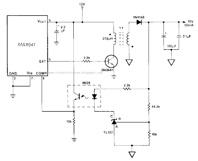
Build a Isolated Dc Dc Converter Wiring diagram Schematic

This Isolated Dc-Dc Converter Circuit Diagram, a TU31 shunt regulator is used to sense the output voltage. The TU31 drives the LED of a 4N28 optocoupler which provides feedback to the MAX641 while maintaining isolation between the input, +12 V, andJhe output, +15 V. ln this  Isolated Dc-Dc Converter Circuit Diagram, the +15 V output is fully regulated with respect to both line and load changes.

 Isolated Dc-Dc Converter Circuit Diagram

Isolated Dc-Dc Converter Circuit Diagram

Read More..