Showing posts with label diagram. Show all posts

Friday, November 7, 2014

Morning Alarm Circuit Diagram Using LDR

Description Circuit showing a morning alarm.Here we have used a switching transistor.When the sun rise up ldr is low resistance so the ldr is conduct and a positive volt coming to the base of the Q1 there for the transistor will switch.This time  the buzzer is ON . Adjust the preset control the intensity of light.
Component Required                Resistor  4.7k preset  , LDR
Read More..

Tuesday, November 4, 2014

Small Single Chip FM Transmitter Circuit Schematic Diagram

Small Single Chip FM Transmitter Circuit Schematic Diagram

The following circuit schematic diagram is the one used for the monophonic FM Transmitter. It is pretty clear seen on the circuit’s schematic that the left and the right signal is mixed before modulate the radio frequency.

Maxim Semiconductor’s MAX2606 is the core of this circuit. It is an integrated circuit which is compact, high-performance intermediate frequency voltage controlled oscillators. The output from this circuit is -21 dBm radiation power, and work with 3 volts power supply, so two small batteries with 1.5 volts each should be enough. You just only need a potentiometer to tune in the frequency within commercial FM broadcast band 88-108 MHz. And that is the best part. The frequency tuning circuitry have been handled by the IC, so you don’t need to bother. External varactor even doesn’t need in this circuit. One of the application that can be used with this circuit, you can extend your mp3/CD player in your room to your portable set around the house. Much more simple than using wires.
Read More..

Monday, November 3, 2014

14W AUDIO AMPLIFIER TDA2030 ELECTRONIC DIAGRAM

14W AUDIO AMPLIFIER TDA2030 ELECTRONIC DIAGRAM

The values of R5 and C8 are worked out from the equations in the datasheet, but I used 1.8k ohm for R5 and 220pF for C8 and they work fine. Diodes should be 1N4001 or similar (make sure you solder them in the right way round).

A good heatsink is important and this should be a large size with good thermal conductivity. When you operate the TDA2030 from the (recommended) split rail power supply, you must insulate the device from the heatsink using a mica washer or similar. With single rail supply, this is not needed.
Read More..

Sunday, November 2, 2014

LOW NOISE WHITE LED DRIVER SYSTEM ELECTRONIC DIAGRAM


LOW NOISE WHITE LED DRIVER SYSTEM ELECTRONIC DIAGRAM

The LM3570 evaluation board has a chip enable pin (active high logic) as well as a PWM (active high logic) pin which allows current sources to be turned on and off without completely disabling the part..The LM3570 is capable of supplying up to 80mA of current split between the regulated current sources and VOUT. The LM3570 comes in National’s LLP-14 package.
Read More..

Thursday, October 30, 2014

Monitoring Acoustic Sensor Circuit Diagram

This is the Monitoring Acoustic Sensor Circuit Diagram. This acoustic sensor was originally developed for an industrial application (monitoring a siren), but will also find many domestic applications. Note that the sensor is designed with safety of operation as the top priority: this means that if it fails then in the worst-case scenario it will not itself generate a false indication that a sound is detected. Also, the sensor connections are protected against polarity reversal and short-circuits. The supply voltage of 24 V is suitable for industrial use, and the output of the sensor swings over the supply voltage range.

Simple Acoustic Sensor Circuit diagram :

simple
Simple Acoustic Sensor Circuit Diagram

The circuit consists of an electret micro-phone, an amplifier, attenuator, rectifier and a switching stage. MIC1 is supplied with a current of 1 mA by R9. T1 amplifies the signal, decoupled from the supply by C1, to about 1 Vpp. R7 sets the collector current of T1 to a maximum of 0.5 mA. The operating point is set by feedback resistor R8. The sensitivity of the circuit can be adjusted using potentiometer P1 so that it does not respond to ambient noise levels. Diodes D1 and D2 recitfy the signal and C4 provides smoothing. As soon as the voltage across C4 rises above 0.5 V, T2 turns on and the LED connected to the collector of the transistor lights. T3 inverts this signal.

If the microphone receives no sound, T3 turns on and the output will be at ground. If a signal is detected, T3 turns off and the output is pulled to +24 V by R4 and R5. In order to allow for an output current of 10 mA, T3’s collector resistor needs to be 2.4 kΩ. If 0.25 W resistors are to be used, then to be on the safe side this should be made up of two 4.7 kΩ resistors wired in parallel. Diode D4 protects the circuit from reverse polarity connection, and D3 protects the output from damage if it is inadvertently connected to the supply.


Author:Engelbert Göpfert - Copyright : Elektor
Read More..

Wednesday, October 29, 2014

Telephone Headgear Circuit Diagram

Acompact, inexpensive and low component count telecom head- set can be constructed using two readily available transistors and a few other electronic components. This circuit is very useful for hands-free operation of EPABX and pager communication. Since the circuit draws very little current, it is ideal for parallel operation with electronic telephone set. 

Telephone

Working of the circuit is simple and straightforward. Resistor R1 and an ordinary neon glow- lamp forms a complete visual ringer circuit. This simple arrangement does not require a DC blocking capacitor because, under idle conditions, the telephone line voltage is insufficient to ionise the neon gas and thus the lamp does not light. Only when the ring signal is being received, it flashes at the ringing rate to indicate an incoming call. The bridge rectifier using diodes D1 through D4 acts as a polarity guard which protects the electronic circuit from any changes in the telephone line polarity. 

Zener diode D5 at the output of this bridge rectifier is used for additional circuit protection. Section comprising transistor T1, resistors R2, R3 and zener diode D6 forms a constant voltage regulator that provides a low voltage output of about 5 volts. Dial tone and speech signals from exchange are coupled to the receiving sound amplifier stage built around transistors T2 and related parts, i.e. resistors R7, R6 and capacitor C5. Amplified signals from collector of transistor T2 are connected to dynamic receiver RT-200 (used as earpiece) via capacitor C7. A condenser microphone, connected as shown in the circuit, is used as transmitter. Audio signals developed across the microphone are coupled to the base of transistor T1 via capacitor C3. Resistor R4 determines the DC bias required for the microphone. After amplification by transistor T1, the audio signals are coupled to the telephone lines via the diode bridge. The whole circuit can be wired on a very small PCB and housed in a medium size headphone, as shown in the illustration. For better results at low line currents, value of resistor R2 may be reduced after testing
Read More..

Saturday, October 18, 2014

Circuit Diagram for 250 W HID Metal Halide Electronic Ballast

Circuit Diagram for 250 W HID Metal Halide Electronic Ballast

The following file is an application note from st.com describing the two stages of electronic ballast for a 250 W HID (high-intensity discharge) metal halide lamp. The ballast is composed of a boost converter (power factor controller PFC) working in fixed OFF time and an inverter composed of a full bridge that drives the lamp at low frequency square wave. The components include a PFC driver, half-bridge drivers, a microcontroller, an auxiliary power supply, a voltage reference, logic parts, an amplifier, comparators, power devices as Power MOSFETs, IGBTs, and fast diodes.


Herein this file you will find detail information regarding 250 W HID lamp description, general circuit description, board description, L6385 high-voltage high and low side driver, ST7LITE39 microcontroller (application pin), auxiliary power supply, TS272 high-performance CMOS dual operational amplifiers, LM119 high-speed dual comparators, 74AC00 QUAD2-input NAND gates, lamp data, PFC section design criteria, full bridge design criteria, experimental results, firmware flowchart, references, and revision history.
Read More..

Friday, October 17, 2014

Simple Park Aid Circuit Diagram

This Park-Aid Circuit Diagram was designed as an aid in parking the car near the garage wall when backing up. LED D7 illuminates when bumper-wall distance is about 20 cm., D7+D6 illuminate at about 10 cm. and D7+D6+D5 at about 6 cm. In this manner you are alerted when approaching too close to the wall. All distances mentioned before can vary, depending on infra-red transmitting and receiving LEDs used and are mostly affected by the color of the reflecting surface.

Black surfaces lower greatly the device sensitivity. Obviously, you can use this circuit in other applications like liquids level detection, proximity devices etc. Circuit operation: IC1 forms an oscillator driving the infra-red LED by means of 0.8mSec. pulses at 120Hz frequency and about 300mA peak current. D1 & D2 are placed facing the car on the same line, a couple of centimeters apart, on a short breadboard strip fastened to the wall. D2 picks-up the infra-red beam generated by D1 and reflected by the surface placed in front of it. The signal is amplified by IC2A and peak detected by D4 & C4. Diode D3, with R5 & R6, compensates for the forward diode drop of D4. A DC voltage proportional to the distance of the reflecting object and D1 & D2 feeds the inverting inputs of three voltage comparators. These comparators switch on and off the LEDs, referring to voltages at their non-inverting inputs set by the voltage divider resistor chain R7-R10.


Park-Aid Circuit Diagram


Park-Aid

Parts:
R1_____________10K 1/4W Resistor
R2,R5,R6,R9_____1K 1/4W Resistors
R3_____________33R 1/4W Resistor
R4,R11__________1M 1/4W Resistors
R7______________4K7 1/4W Resistor
R8______________1K5 1/4W Resistor
R10,R12-R14_____1K 1/4W Resistors
C1,C4___________1µF 63V Electrolytic or Polyester Capacitors
C2_____________47pF 63V Ceramic Capacitor
C3,C5_________100µF 25V Electrolytic Capacitors
D1_____________Infra-red LED
D2_____________Infra-red Photo Diode (see Notes)
D3,D4________1N4148 75V 150mA Diodes
D5-7___________LEDs (Any color and size)
IC1_____________555 Timer IC
IC2___________LM324 Low Power Quad Op-amp
IC3____________7812 12V 1A Positive voltage regulator IC

Circuit modification:
A circuit modification featuring an audible alert instead of the visual one is available here: Park-Aid Modification

Notes:
  • Power supply must be regulated (hence the use of IC3) for precise reference voltages. The circuit can be fed by a commercial wall plug-in adapter, having a DC output voltage in the range 12-24V.
  • Current drawing: LEDs off 40mA; all LEDs on 60mA @ 12V DC supply.
  • The infra-red Photo Diode D2, should be of the type incorporating an optical sunlight filter: these components appear in black plastic cases. Some of them resemble TO92 transistors: in this case, please note that the sensitive surface is the curved, not the flat one.
  • Avoid sun or artificial light hitting directly D1 & D2.
  • If your car has black bumpers, you can line-up the infra-red diodes with the (mostly white) license or number plate.
  • It is wiser to place all the circuitry near the infra-red LEDs in a small box. The 3 signaling LEDs can be placed far from the main box at an height making them well visible by the car driver.
  • The best setup is obtained bringing D2 nearer to D1 (without a reflecting object) until D5 illuminates; then moving it a bit until D5 is clearly off. Usually D1-D2 optimum distance lies in the range 1.5-3 cm.
  • If you are needing a simpler circuit of this kind driving a LED or a relay, click Infra-red Level Detectorv
Read More..

Thursday, October 16, 2014

Simple 0 50V 2A Bench Power Supply Circuit Diagram

I use the lm10 IC because it has a reference voltage and that’s useful for dc power supply. With two ICs can take different output voltage and amperage. This circuit is protected from short circuit.P2 is for controlling the current at the range of 0-2A. Stabilize the output voltage with R4 on negative pin on op-amp and with R2 & P1 on positive pin. 

0-50V 2A Bench Power Supply Circuit Diagram

Simple
 
 Op-amp output controls T1 that not let ripple of voltage.T1 increase or decrease ampere of R6 and control the voltage of T5 & T4. Pin 1 is the reference voltage and reference voltage is losing some voltage on R1 that has 100uA . This current passes through P1 too.
Vlose p1=100uA*Rp1

This lose voltage regulate output voltage rate of output current is compare between reference voltage of P3 and lose voltage on R11.T3 is protecting short circuit with R11. For reduce out put voltage to 0v should parallel one resistor 470 ohm in out put. Minimum voltage is 0.4v. The maximum output voltage is fixed with R1b and should not become over of 50v. Therefore your transformer should give 36V, 3A with 4700uF capacitor. T6, T5, T7 need heatsilk.

Simple


R1a = 2,2 K
R1b = read the text
R2 = 10 K
R3, R7 = 3.3 k
R4 = 390 Ohm
R5 = 47 K
R6 = 3.3 K 1Watt
R8 = 180 Ohm
R9, R10 = 0.47 Ohm 3Watt
R11 = 0.075 Ohm 2Watt
R12 = 470 Ohm
P1 = 500K liner potentiometer
P2 = 4.7 K potentiometer
P3 = 10 K potentiometer
C1 = 1nF
C2 = 10nF
C3 = 22nF
C4 = 47mF 63v electrolytic
C5 = 4700mF 80v electrolytic
T1, T2 = BC161
T3, T4 = BD141
T5 = BD241
T6, T7 = 2V3055
D1, D2 = 1N4148
D3, D4 = 1N4001
IC1, IC2 = LM10C
Read More..

Wednesday, October 15, 2014

Simple Frequency Voltage Converter Circuit Diagram

This is the simple frequency voltage converter circuit diagram. Teledyne Semiconductor`s Type TSC9402 is a versatile IC. Not only can it convert voltage into frequency, but also frequency into voltage. It is thus eminently suitable for use in an add-on unit for measuring frequencies with a multimeter. 

Only a few additional components are required for this.. Just one calibration point sets the center of the measuring range (or of that part of the range that is used most frequently). The frequency-proportional direct voltage at the output (pin 12—amp out) contains interference pulses at levels up to 0.7 V. If these have an adverse effect on the multimeter, they can be suppressed with the aid of a simple RC network. 

The output voltage, U0, is calculated by: tfo=C/rei(Ci + 12 pF) R2fm Because the internal capacitance often has a greater value than the 12 pF taken here, the formula does not yield an absolute value. The circuit has a frequency range of dc to 10 kHz. At 10 kHz, the formula gives a value of 3.4 V. The circuit draws a current of not more than 1 mA.

Frequency Voltage Converter Circuit Diagram

Read More..

Monday, October 13, 2014

Digital Ignition System Wiring Diagram Jaguar XJS

Jaguar The 1992 Jaguar XJS ignition system uses a digital microprocessor-controlled system that eliminates vacuum and mechanical advance controls. The microprocessor contains ignition timing with precise timing for engine speeds, loads and modes of operation. This system (located in the ECU), receives inputs from engine sensors to program the necessary ignition timing. The crankshaft position and engine speed inputs are necessary for the engine to start.

The following schematic shows the 1992 Jaguar XJS Digital Ignition System Wiring Diagram.
Read More..

Sunday, October 5, 2014

schematic diagram of Buick Allure Ignition Coil Wire Set and Parts

Buick
Here is a typical schematic diagram of the 2008 Buick Allure Ignition System Parts and Components Assembly.
1. PCM
2. Camshaft sensor
3. Crankshaft sensor
4. Crankshaft sensor Shield
5. Knock sensor
6. Ignition module
7. Ignition module Bracket
8. Ignition coil
9. Ignition coil Seal
10. Plug wire set
11. Spark plug
Read More..

Thursday, October 2, 2014

12 VDC-220 VAC 50W Power Inverter Circuit

12 VDC-220 VAC 50W Power Inverter Circuit

The ability advocate ambit is aimed to catechumen 12 VDC to 220 VAC and the action accepted as inverter. By inverting action will aftermath a 50W ability advocate that would accumulation altered baby appliances.
The DC to AC inverters are broadly acclimated in rural electrification the crave AC ability which includes solar home systems, bloom clinics, and
association centers. Ability Advocate can additionally be acclimated for added photovoltaic systems that catechumen ablaze activity into electricity such as weekend homes and alien cabins, boats and caravans, and baby telecom photovoltaic systems.
Power Advocate Ambit Explanation
The ability advocate ambit is constituted by the oscillator, annular the IC1, one affiliate IC2, one ambiguous multivibrator IC3, which accord in the achievement balanced aboveboard arresting of abundance 50HZ, chase a absorber date with Fet Q1-2, the drive date Q3-4 and the ability date Q4-5, the ability transistors Q5-6, should they are placed in heatsink.
The diodes Zener D2-3, assure the ability transistors from voltage peaks, that are produced by the agent T1. Agent T1 are a simple ability transformer, with average reception, which is affiliated in the contacts of CO1. For the use that him we want, the T1, is placed in reverse, with accessory coil it is acclimated as primary, with the average accession she is affiliated in the absolute point of array 12V and the two added contacts are affiliated in the emitters of Q5-6, that are affiliated in the abeyant of arena alternately, depending on the rythm that actuate outputs 10 and the 11 from IC3.
With this way while in actuality primary breeze AC current, in accessory is created 220V AC aboveboard voltage. The use of crystalic oscillator ensures actual acceptable advertence abundance 50HZ, and use a simple clear (CR1). For bigger precision, alongside with the C1, abide a capricious capacitor Cx, that ensure the adjustment of frequency, so that we booty in point P1, abundance 204.8 KHZ.
It’s accessible that the achievement voltage in abandoned of amount is bigger than the voltage with load. Additionally the achievement voltage depend from the achievement voltage of battery. Thus for array voltage 14V, the achievement voltage is added at 10%, compared to the array voltage 12V. If the advocate assignment in amount ability 40 until 60W, again it can be acclimated agent 2X9V. Various prices of output, for array voltage 12V and agent 2X10V,
Power Converter Parts List
Resistor
R1=10Mohms
R2=100ohms
R3=1.2Kohms
R4=560Kohms
R5-6=2.2Kohms
R7-8=56 ohms 5W
Capacitor
CX=22pF trimmed capacitor
C1-2=22pF ceramic
C3=8.2nF 100V MKT C4=10uF 16V
C5=47uF 16V
C6=470nF 400V
Diode
D1=5V6 0.4W
D2-3=47V 1W
Transistor
Q1-2=BS170
Q3-4=BD139
Q5-6=BD249
Integrated Circuit
IC1=4060
IC2=4013
IC3=4047
Crystal
CR1=3.2768 MHZ crystal
Transformer-Fuse
T1=220Vac/2X10V 2X2.2A
F1=5A Fuse
F2=0.25A Fuse
Inductor
L1=1H smoothing choke
Read More..

Wednesday, October 1, 2014

Super Zener Diode Circuit Diagram

  1. Although the temperature coefficient of the super zener circuit can be optimized by careful dimensioning of the components, there exists a still better way for making a precision voltage reference.
  2. It is generally known that the accuracy of measurements in electronic circuits is mainly a function of the stability and reliability of the reference against which the unknown quantity is compared.
  3. The zenerdiode in Fig. l is a usable reference device for , applications where the above i three parameters are not subject to appreciable variation.
  4. The "super zener" in Fig.2 features excellent stability and is hardly affected by variations in the supply voltage and the load current.
  5. The term band gap refers to the difference between two discrete energies of the outer four electrons in a semiconductor atom. Electrons in the highest energy band contribute to the conduction of the material.
  6. There fore, everything feasible should be done to maintain the stability of the reference, i.e., counteract the adverse effects of variations in the ambient temperature, supply voltage, and load current. 
Super Zener Diode Circuit Diagram


Read More..

Sunday, September 21, 2014

Mercedes Explanation Fuse Box Year Benz 2001 CLK 320 Diagram

Fuse Box Mercedes Benz 2001 CLK 320 Diagram - Below is Fuse Box Mercedes Benz 2001 CLK 320 Diagram.

Fuse Box Mercedes Benz 2001 CLK 320 Diagram


Fuse
Fuse

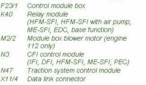
Fuse Panel Layout Diagram Parts: control module box, relay module, air pump, blower motor, CFI control module, traction system control module, data link connector.
Read More..

Fuse Box Ford 2001 Escape Under Hood Diagram

Fuse Box Ford 2001 Escape Under Hood Diagram - Here are new post for Fuse Box Ford 2001 Escape Under Hood Diagram.

Fuse Box Ford 2001 Escape Under Hood Diagram


Fuse
Fuse

Fuse Panel Layout Diagram Parts: horn, headlamp, high beam relay, EEC.
Read More..

Mercedes Explanation Fuse Box Year 1989 230 Fuel Injection Diagram

Fuse Box Mercedes 1989 230 Fuel Injection Diagram - Below is Fuse Box Mercedes 1989 230 Fuel Injection Diagram.

Fuse Box Mercedes 1989 230 Fuel Injection Diagram


Fuse
Fuse

Fuse Panel Layout Diagram Parts: gear start relay, combination relay, power seat relay, auxiliary fan, preresistor relay, headlamp washer relay, auxiliary fuse holder, power seat diode, parking brake, electronic accelerator, exterior lamp failure monitoring unit, air injection relay, power window relay, convenience relay, seat belt warning relay.
Read More..

Saturday, September 20, 2014

Fuse Box BMW R1150GS 2000 Diagram

Fuse Box BMW R1150GS 2000 Diagram - Here are new post for Fuse Box BMW R1150GS 2000 Diagram.

Fuse Box BMW R1150GS 2000 Diagram


Fuse
Fuse

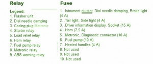
Fuse Panel Layout Diagram Parts: Side light, Driver information display, ABS warning relay, Flasher unit, Dial needle damping, Socket, Horn, Motronic, Coding plug Motronic, Horn relay, Fuel pump relay, Motronic relay, Brake light, Tail light, Starter relay, Load relief relay, Diagnostic connector, Fuel pump, Heated handles, Istrument cluster, Dial needle damping,
Read More..

Fuse Box Acura 1999 CL Diagram

Fuse Box Acura 1999 CL Diagram - Here are new post for Fuse Box Acura 1999 CL Diagram.

Fuse Box Acura 1999 CL Diagram


Fuse
Fuse

Fuse Panel Layout Diagram Parts: daytime running light, starter signal, heater control, AC clutch, ignition coil, spare fuse, wiper/washer, master light, clock security, spare fuse, ECU, cruise control, fan timer, SRS, fuel pump, back up light, turn signal, cooling fan relay, power mirror, mirror heater, spare fuse, ABS motor, ABS unit, Radio.
Read More..

Friday, September 19, 2014

Fuse Box BMW Z4 Coupe 2007 Diagram

Fuse Box BMW Z4 Coupe 2007 Diagram - Here are new post for Fuse Box BMW Z4 Coupe 2007 Diagram.

Fuse Box BMW Z4 Coupe 2007 Diagram


Fuse
Fuse

Fuse Panel Layout Diagram Parts: turn indicator, hazard warning flasher, comp. light, low beam headlight, airbag, high beam headlight, brake light, side light, ASC/DSC, CD charger, central locking system, cigar lighter, clutch switch, interior and luggage,
Read More..