Showing posts with label audio. Show all posts

Wednesday, November 5, 2014

3 Channel Audio Splitter

This circuit is suitable to amplify and distribute the audio signals. The input audio signal is applied to the J1 and after passing through the P1, It is buffered and amplified by the IC1 prepared to redistribute. It has 3 outputs to drive 3 audio lines with 300 ohms impedance.


3 Channel Audio Splitter Circuit Diagram :


Parts:

J1 = RCA Socket (See Notes)
P1 = 100K-Potentiometre
R* = 10K-100K
R1 = 560K
R2 = 1K
R3 = 2.2K
R4 = 2.7K
R5 = 2.7K
R6 = 330R
R7 = 330R
R8 = 330R
C1 = 100uF-25V
C2 = 100uF-25V
C3 = 100uF-25V
D1 = BZX79C18
D2 = BZX79C18
Q1 = BC337
Q2 = BC327
IC1 = NE5532-34

Notes:
  • J1 will be RCA Audio input female socket.
  • R* is on your choice it can be choose between 10K to 100K resistor.
  • Output capacitor’s value is between 100uf to 470uf and power handling is 25V to 50V.
  • You can power up this circuit via +12V/-12V regulated supply but you have to remove following parts Q1-Q2-C2-C3-D1-D2.
  • Maximum power ratings +35V/-35V
Read More..

Automatic Switch For Audio Power Amplifier

Automatic Switch For Audio Power Amplifier. Circuit of an automatic switch for audio power amplifier stage is presented here. The circuit uses stereo preamplifier output to detect the presence of audio to switch the audio power amplifier on only when audio is present.

The circuit thus helps curtail power wastage. IC1 is used as an inverting adder. The input signals from left and right channels are combined to form a common signal for IC2, which is used as an open loop comparator. IC3 (NE556) is a dual timer. Its second section, i.e., IC3(b), is configured as monostable multivibrator. Output of IC3(b) is used to switch the power amplifier on or off through a Darlington pair formed by transistors T1 and T2. IC3(a) is used to trigger the monostable multivibrator whenever an input signal is sensed.

Switch For Audio Power Amplifier Circuit Diagram:

Amplifier-Circuit-Diagram

Under ‘no signal’ condition, pin 3 of IC2 is negative with respect to its pin 2. Hence the output of IC2 is low and as a result output of IC3(a) is high. Since there is no trigger at pin 8 of IC3(b), the output of IC3(b) will be low and the amplifier will be off. When an input singal is applied to IC1, IC2 converts the inverted sum of the input signals into a rectangular waveform by comparing it with a constant voltage which can be controlled by varying potentiometer VR1. When the output of IC2 is high, output pin 5 of IC3 goes low, thus triggering the monostable multivibrator. As soon as the audio input to IC1 stops, pin 5 of IC3 goes high and pin 1 of IC3 discharges through capacitor C3, thus resetting the monostable multivibrator.

Hence, as long as input signals are applied, the amplifier remains ‘on.’ When the input signals are removed, i.e., when signal level is zero, the amplifier switches off after the mono flip-flop delay period determined by the values of resistor R8 and capacitor C3. If no input signals are sensed within this time, the amplifier turns off—else it remains on. Power supply for the circuit can be obtained from the power supply of the amplifier. Hence, the circuit can be permanently fitted in the amplifier box itself. The main switch of the amplifier should be always kept on. Resistors R1 and R2 are used to divide single voltage supply into two equal parts.

Capacitors C1 and C2 are used as regulators and also as an AC bypass for input signals. Diode D1 is used so that loading fluctuations in power amplifier do not affect circuit regulation. Transisitor T2 acts as a high voltage switch which may be replaced by any other high voltage switching transistor satisfying amplifier current requirements. Value of resistor R10 should be modified for large current requirement. The LED glows when the amplifier is on. The circuit is very useful and relieves one from putting the amplifier on and off every time one plays a cassette or radio etc. 


Read More..

Tuesday, November 4, 2014

LM4990 2 Watt Audio Power Amplifier with Selectable Shutdown Logic Level

The LM4990 is an audio power amplifier primarily designed for demanding applications in mobile phones and other portable communication device applications. It is capable of delivering 1.25 watts of continuous average power to an 8Ω BTL load and 2 watts of continuous average power (LD and MH only) to a 4Ω BTL load with less than 1% distortion (THD+N+N) from a 5VDC power supply. Boomer audio power amplifiers were designed specifically to provide high quality output power with a minimal amount of external components. The LM4990 does not require output coupling capacitors or bootstrap capacitors, and therefore is ideally suited for mobile phone and other low voltage applications where minimal power consumption is a primary requirement.


2  2 Watt Audio Power Amplifier with Selectable Shutdown Logic Level

The LM4990 features a low-power consumption shutdown mode. To facilitate this, Shutdown may be enabled by either logic high or low depending on mode selection. Driving the shutdown mode pin either high or low enables the shutdown pin to be driven in a likewise manner to enable shutdown. The LM4990 contains advanced pop & click circuitry which eliminates noise which would otherwise occur during turn-on and turn-off transitions. The LM4990 is unity-gain stable and can be configured by external gain-setting resistors.
 Features


  • Available in space-saving packages: LLP, Exposed-DAP TSSOP, MSOP, and ITL
  • Ultra low current shutdown mode
  • Improved pop & click circuitry eliminates noise during turn-on and turn-off transitions
  • 2.2 - 5.5V operation
  • No output coupling capacitors, snubber networks or bootstrap capacitors required
  • Unity-gain stable
  • External gain configuration capability

  • User selectable shutdown High or Low logic Level
    Key Specification
    Improved PSRR at 217Hz & 1KHz  62dB
    Power Output at 5.0V, 1% THD+N, 4Ω (LD and MH only) 2W (typ)
    Power Output at 5.0V, 1% THD+N, 8Ω 1.25W (typ)
    Power Output at 3.0V, 1% THD+N, 4Ω 600mW (typ)
    Power Output at 3.0V, 1% THD+N, 8Ω 425mW (typ)
    Shutdown Current 0.1µA (typ)

    Applications

    • Mobile Phones
    • PDAs
    • Portable electronic devices
    Datasheets


    Read More..

    Monday, November 3, 2014

    14W AUDIO AMPLIFIER TDA2030 ELECTRONIC DIAGRAM

    14W AUDIO AMPLIFIER TDA2030 ELECTRONIC DIAGRAM

    The values of R5 and C8 are worked out from the equations in the datasheet, but I used 1.8k ohm for R5 and 220pF for C8 and they work fine. Diodes should be 1N4001 or similar (make sure you solder them in the right way round).

    A good heatsink is important and this should be a large size with good thermal conductivity. When you operate the TDA2030 from the (recommended) split rail power supply, you must insulate the device from the heatsink using a mica washer or similar. With single rail supply, this is not needed.
    Read More..

    Wednesday, October 29, 2014

    STK4050 Audio Amplifier with 200W

    Overview
    The project is based around the hybrid integrated circuit STK4050 manufactured by Sanyo to build a low noise mono audio amplifier with complete high quality.
    Explanation The project has a maximum output power of 200W while incorporating a volume control. The power supply used in the circuit is an on-board type and because of this, only a center tapped transformer is needed for the powering of the circuit. The sound has a very good quality and it can be proven when used in home theaters, in computers, and other audio equipments which can also be used as subwoofer amplifier.
    For thin-type audio sets, it can be considered as a compact package. The heat generated in thin-type audio sets is being dispersed easily with a good heatsink design. There may be case where a shock noise may be encountered especially during switch ON and switch OFF. This can be reduced by providing a constant current circuit. The design of the circuit can be tailored for reducing occurrence of thermal shutdown, short circuit protection for loads, shock noise muting from external power supply.
    The load resistance should have 8 Ohms value with 55K Ohms input impedance.


     Modifikasi STK 4050

    Read More..

    Wednesday, October 15, 2014

    Build a 25W Bridge Audio Amplifier with TDA2005

    This is the 25W bridge audio amplifier built using single power IC TDA2005. Actually, the TDA2005 is a stereo power amplifier chip. It has two input channels and two output channel and delivers about 10W power output for each channel, since it connected in bridge mode then it will delivering up to 25W audio output. Take a note that the speaker terminals should not conected to the ground and mount the IC on the heatsink to prevent overheating.

     25W Bridge Audio Amplifier with TDA2005 Circuit Diagram

     
    Parts List:
    R1 = 120K?
    R2,5,6 = 1K?
    R3,4 = 12?
    R7,8= 1?
    C1,5,7 = 220uF/25V
    C2,10,11 = 100nF
    C3,4 = 2.2uF/25V
    C6,8 = 100uF/25V
    C9 = 10uF/25V
    IC1 = LM2005M / TDA2005
    Read More..

    Tuesday, September 9, 2014

    600W Audio Amplifier Wiring diagram Schematic

    The 600W Audio Amplifier Circuit Diagram is based around {LM4702}manufactured by NATIONAL semiconductors&{MJ11029-MJ11028} by ON semiconductors It is a high fidelity audio power amplifier. Designed for demanding consumer and pro-audio applications. You can also use this schema with AV receivers, Audiophile power amps, Pro Audio High voltage industrial applications etc Amplifier output power maybe scaled by changing the supply voltage and number of output devices. The schema includes thermal shutdown schemary that activates when the die temperature exceeds 150°c. CIRCUIT’s mute function, when activated, mutes the input drive signal and forces the amplifier output to a quiescent state.

     Simple 600W Audio Amplifier Circuit Diagram

    Simple

    Power:
    Maximum Output power @ 8ohms : 300watt
    Absolute max power supply voltage :±38V to ±40V
    Recommended power supply voltage :±30V to ±35V
    Read More..

    Monday, September 8, 2014

    Telephone line Based Audio Muting and Light On Circuit

    Telephone line Based Audio Muting and Light-On Circuit. Very often when enjoying music or watching TV at high audio level, we may not be able to hear a telephone ring and thus miss an important incoming phone call. To overcome this situation, the schema presented here can be used. The schema would automatically light a bulb on arrival of a telephone ring and simultaneously mute the music system/TV audio for the duration the telephone handset is off-hook. Lighting of the bulb would not only indicate an incoming call but also help in locating the telephone during darkness.
    .
    Circuit diagram :
    Telephone Telephone line Based Audio Muting and Light-On Circuit Diagram 
    .
    On arrival of a ring, or when the handset is off-hook, the inbuilt transistor of IC1 (opto-coupler) conducts and capacitor C1 gets charged and, in turn, transistor T1 gets forward biased. As a result, transistor T1 conducts, causing energisation of relays RL1, RL2, and RL3. Diode D1 connected in antiparallel to inbuilt diode of IC1, in shunt with resistor R1, provides an easy path for AC current and helps in limiting the voltage across inbuilt diode to a safe value during the ringing. (The RMS value of ring voltage lies between 70 and 90 volts RMS.) Capacitor C1 maintains necessary voltage for continuously forward biasing  transistor T1 so that the relays are not energised during the negative half cycles and off-period of ring signal. Once the handset is picked up, the relays will still remain energised because of low impedance DC path available (via cradle switch and handset) for the in-built diode of IC1. 

    After completion of call when handset is placed back on its cradle, the low-impedance path through handset is no more available and thus relays RL1 through RL3 are deactivated. As shown in the figure, the energised relay RL1 switches on the light, while energisation of relay RL2 causes the path of TV speaker lead to be opened. (For dual-speaker TV, replace relay RL2 with a DPDT relay of 6V, 200 ohm.) Similarly, energisation of DPDT relay RL3 opens the leads going to the speakers and thus mutes both audio speakers. Use ‘NC’ contacts of relay RL3 in series with speakers of music system and ‘NC’ contacts of RL2 in series with TV speaker. Use  ‘NO’ con-tact of relay RL1 in series with a bulb to get the visual indication. 


    Author : Dhurjati Sinha - Copyright : EFYmag
    Read More..

    Low Power Wireless Audio Power Amplifier

    Battery-Powered portable unit, Suitable for all type Televisions

    Using this low-cost project one can reproduce audio from TV without disturbing others. It does not use any wire connection between TV and Loud Speaker. In place of a pair of wires, it uses invisible infra-red light to transmit audio signals from TV to Loud speakers, Without using any lens a range of up to 6 meters is possible. Range can be extended by using lenses and reflectors with IR sensors comprising transmitters and receivers.

    Transmitters operation:

    IR transmitter uses two-stage transistor amplifier to drive two series-connected IR LEDs. An audio output transformer (T1) is used (in reverse) to couple audio output from TV to the IR transmitter. Transistors Q1 and Q2 amplify the audio signals received from TV through the audio transformer. Low impedance output windings (lower gauge or thicker wires) are used for connection to TV side while high-impedance windings are connected to IR transmitter. This IR transmitter can be powered from a 9V mains adapter or a 9V battery. Red LED (D1) in transmitter schema functions as a Zener diode (0.65V) as well as supply-on indicator.

    Transmitter diagram:
     wireless audio power amplifier transmitter schematic schema diagram
    Wireless Audio Power Amplifier Transmitter Circuit Diagram

    Receivers operation:
    IR receiver uses popular op-amp IC µA741 and audio-frequency amplifier IC LM386 along with phototransistor L14F1 (Q3) and some discrete components. The sound generated by TV set is transmitted through IR LEDs, received by phototransistor Q3 and fed to pin 2 of IC µA741 (IC1). Its gain can be varied using potmeter P2. The output of IC µA741 is fed to IC LM386 (IC2) via capacitor (C7) and potmeter P3. The sound produced is heard through the receiver’s loudspeaker. Potmeter P3 is used to control the volume of loudspeaker SPKR (8-ohm, 1W).

    Receiver diagram:
     wireless audio power amplifier reciever schematic schema diagram
    Wireless Audio Power Amplifier Transmitter Circuit Diagram

    Parts:

    P1 = 10K
    P3 = 10K
    P2 = 1M

    R1 = 4.7K
    R2 = 22K
    R3 = 100R
    R4 = 10R-1W
    R5 = 10K
    R6 = 10K
    R7 = 15K
    R8 = 15K
    R9 = 100K
    R10 = 680R-1W
    R11 = 1K
    R12 = 10R-1W

    C1 = 220uF-25V
    C2 = 220uF-25V
    C3 = 10uF-25V
    C4 = 220uF-25V
    C5 = 220uF-25V
    C6 = 100nF-63V
    C7 = 100nF-63V
    C8 = 100nF-63V
    C9 = 100nF-63V

    D1 = Red LED
    D2 = IR LEDs
    D3 = IR LEDs

    Q1 = BC547
    Q2 = BD140
    Q3 = L14F1

    IC1 = uA741 Opamp
    IC2 = LM386

    J1 = Audio input Jack
    T1 = Audio Transformer
    SPKR = 1W-8ohm
    Read More..

    Sunday, September 7, 2014

    5 8 Watt Audio Power Amplifier

    This schema use TA7222AP to amplifiers audio signal .The price only $0.99 and can provide 5.8 watt with Muting Control.Power supply can use for 8-12Vdc it is a good idea to use for car audio power amp , coin-op machine game, security system etc.


    Fig 1. TA7222AP pin out


    Pin Name Description
    1 Vcc Supply Voltage
    2 RR Ripple Reject
    3 MC Muting control
    4 OP AF Signal Input
    5 FB FB Filter
    6 GA Gain adjust
    7 GND Ground
    8 GND Ground
    9 OP AF Output
    10 BS BootStrap


    Fig 2. schematic for 5.8 watt audio power amplifier
    Read More..

    Saturday, September 6, 2014

    50W car audio amplifier schematic circuits

    50WCar power amplifier uses SI1050GL IC as the main amplifier. The output power 50 Watt 8 ohm mono impedance. Up to 25 Volt DC voltage. with source voltage of this amplifier car battery has to work.

    Read more
    Read More..

    High and quality audio power amplifier with MJ15024G and MJ15025G

    Spesification of this amplifier is high enough , and require a lot of expense to make this super-power amplifier. In the transformer using 20A and manufactered / branded ERA , ERA trafo is one of the best transformer , in addition to the power amplifier as well as power supply adapter , regulator , stabilizer , charger , etc. Because copper is intact , a strong iron and did not issue a frequency so that when the amplifier is turned on , output sound amplifier no buzzing. So if you in choosing a transformer , do not hesitate to use the transformer branded ERA.
    hightransistor 
    Above and below the picture is the end of the amplifier circuit, so-called booster amplifier. Picture above using 14 pairs of transistor MJ15025G and his partner MJ15024G . Transistor price range of $5 - $6 , has power output of 250W on each transistor , for more details , see datasheet of each transistor.
    Click to view larger
    Installed transistor with resistor but still a mess
    Transistors MJ5025G and MJ15024G very fith with power amplifier 300 Watt subwoofer , 450 Watt , 600W , 750 Watt , 1050 Watt , 1200 Watt , and higher. The buffer and its driver using transistor not ic. For power schematic diagram can be found here.
    Read More..

    Friday, September 5, 2014

    Audio Controlled Mains Switch

    Audio Controlled Mains Switch Circuit Diagram. It is often useful for audio or video equipment to be switched off automatically after there has been no input signal for a while. The function of the on-off switch in such equipment is then taken over by switch S2 in the accompanying diagram. It remains, however, possible to  switch off manually by means of Si. Automatic  switch-off occurs after there has been no input  signal for about 2 minutes: this delay makes it possible for a new record or cassette to be placed in the  relevant machine.
     
    The audio input to the proposed schema may be  taken from the output of the relevant TV set, amplifier, or whatever. The input earth is held at + 6 V  with respect to the schema earth by potential divider  Ri-R2-R3-R4. The two 741s function as comparators: the output of ICi goes high when the in- put signal is greater than + 50 mV, whereas the out- put of IC2 goes high when the input signal  becomes more negative than -50 mV. Resistors  R6, R7, and R8 form an OR gate that drives transistor Ti. If the output of either ICi or IC2 is logic  1, Ti conducts.
     
    Circuit diagram :

     audio controlled mains switch circuit diagram
     
    Audio Controlled Mains Switch Circuit Diagram

    The 555  operates as a retrigger able monostable,  whose period is determined by Rio and Ci. The  device is triggered when its pin 2 is earthed by the  closing of S2. Its output, pin 3, then remains high  for 1 to 2 minutes, depending on the leakage cur- rent of the 555. The monostable resets itself as soon  as the potential across Ci exceeds a certain value.  As long as there is an input signal to the schema, Ti conducts and Ci remains uncharged. As soon as  the audio signal ceases, Ti switches off, and Ci  charges until the potential across it is sufficient to  reset the 555. The monostable may also be reset by  closing Si, which connects pin 6 of the 555 to + 12 V.
     
    Audio-Controlled-Mains-Switch

    When IC3 is reset, Ci is discharged via its pin 7. Resistor Rrn serves as protection, because without it Ti could short-schema the supply lines. When the output of IC3 goes high, T2 conducts,  the relay is energized, and the relay contacts switch on the mains voltage as appropriate. To counter the induced potential when the relay contacts close, which could damage T2, diode Di has been connected in parallel with the relay coil.
    Read More..

    Thursday, September 4, 2014

    6 12 Volt audio amplifier circuits

    6
    The above is an amplifier circuit using supply voltages from 6 volts DC to 12 Volt DC. Power output of the amplifier is quite low with only 1 Watt 8 ohm impedance. You can apply this to the audio signal amplifiers that require strengthening are not so large as in the pocket radio.
    Read more
    Read More..

    Wednesday, September 3, 2014

    Audio Surround Decoder Circuit

    The circuit schematic drawings Surround Audio Decoder and its components and how to make it ,Audio surround decoder circuit. Surround sound quality is the process of adding the audio source by increasing the number of speakers. This is done by producing audio multitracking in a way that can be issued on a multichannel speaker.


    Basically surround adopt an existing stereo system. The system uses a two-speaker stereo is right speaker and left speaker. With two speakers will be three-dimensional effect of the sound issued. With the surround, which generated three-dimensional effect was more extensive than in stereo. This is because the surround speakers that use more than two pieces. In addition to supporting the three-dimensional effects, stereo field theory is also noteworthy to organize the arrangement of sounds based on the type of sound produced.

    Component List :

    R1-2-7-8-12-13-18-19-20 : 47Kohm
    R3-4-5-6-21-22-34-35    : 10Kohm
    R9-10-11-14-15-16-17    : 15Kohm
    R23-24-25-33-36         : 100ohm
    R26-27-28-31-32         : 100Kohm
    R29-30                  : 5.6Kohm
    C1-8                    : 47uF/25V
    C2-7-9-14-23            : 47nF
    C3-6                    : 1uF/100V
    C4-5-10                 : 33pF
    C11-12-15               : 10uF/25V
    C13                     : 82nF
    C16                     : 18pF
    C17                     : 100pF mini adjustable capacitor
    C18                     : 2.2nF
    C19                     : 4.7uF/25V
    C20                     : 100nF
    C21                     : 10nF
    C22                     : 180pF
    C24                     : 150nF
    RV1-RV2                 : 2 X 10Kohm  Log. pot.
    RV3-4                   : 10K Log pot.
    D1                      : 1N4148
    IC1-6                   : TL072
    IC2-3                   : TL074
    IC4                     : MN3101
    IC5                     : MN3004


    Surround effects can only be listened to speakers who have more than two channels. Surround is a technique commonly used in todays films that utilize multichannel speakers. Surround allows voice can move from side to side, is a moving side to side is to move from one speaker to another speaker. To create three-dimensional sound effects you can use a series of audio surround decoder.
    Read More..

    Tuesday, September 2, 2014

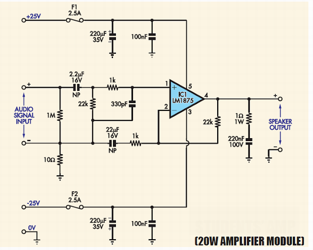
    LM1875 AUDIO AMPLIFIER 20W

    LM1875general description:

    The LM1875 is a monolithic power amplifier offering very low distortion and high quality performance for consumer audio applications. The LM1875 delivers 20 watts into a 4Ω or 8Ω load on ±25V supplies. Using an 8Ω load and ±30V supplies, over 30 watts of power may be delivered. The amplifier is designed to operate with a minimum of external components. Device overload protection consists of both internal current limit and thermal shutdown.The LM1875 design takes advantage of advanced circuit techniques and processing to achieve extremely low distortion levels even at high output power levels. Other outstanding features include high gain, fast slew rate and a wide power bandwidth, large output voltage swing, high current capability, and a very wide supply range. The amplifier is internally compensated and stable for gains of 10 or greater.

    LM1875 amplifier circuit:

    LM1875 power supply diagram:

    LM1875 pcb layout:

    LM1875 project review:


    Read More..

    Saturday, August 30, 2014

    Audio Controlled Mains Switch Wiring diagram Schematic

    It is often useful for audio or video equipment to be switched off automatically after there has been no input signal for a while. The function of the on-off switch in such equipment is then taken over by switch S2 in the accompanying diagram. It remains, however, possible to  switch off manually by means of Si. Automatic  switch-off occurs after there has been no input  signal for about 2 minutes: this delay makes it possible for a new record or cassette to be placed in the  relevant machine.
     
    The audio input to the proposed schema may be  taken from the output of the relevant TV set, amplifier, or whatever. The input earth is held at + 6 V  with respect to the schema earth by potential divider  Ri-R2-R3-R4. The two 741s function as comparators: the output of ICi goes high when the in- put signal is greater than + 50 mV, whereas the out- put of IC2 goes high when the input signal  becomes more negative than -50 mV. Resistors  R6, R7, and R8 form an OR gate that drives transistor Ti. If the output of either ICi or IC2 is logic  1, Ti conducts.
     
    Audio Controlled Mains Switch  Circuit diagram :

    Audio 
    Audio Controlled Mains Switch Circuit Diagram

    The 555  operates as a retrigger able monostable,  whose period is determined by Rio and Ci. The  device is triggered when its pin 2 is earthed by the  closing of S2. Its output, pin 3, then remains high  for 1 to 2 minutes, depending on the leakage cur- rent of the 555. 

    The monostable resets itself as soon  as the potential across Ci exceeds a certain value.  As long as there is an input signal to the schema, Ti conducts and Ci remains uncharged. As soon as  the audio signal ceases, Ti switches off, and Ci  charges until the potential across it is sufficient to  reset the 555. The monostable may also be reset by  closing Si, which connects pin 6 of the 555 to + 12 V.
     
    Audio-Controlled-Mains-Switch


    When IC3 is reset, Ci is discharged via its pin 7. Resistor Rrn serves as protection, because without it Ti could short-schema the supply lines. When the output of IC3 goes high, T2 conducts,  the relay is energized, and the relay contacts switch on the mains voltage as appropriate. To counter the induced potential when the relay contacts close, which could damage T2, diode Di has been connected in parallel with the relay coil.


    Source by : Streampowers
    Read More..

    LM317 Simple Audio Amplifier Circuits

    You most likely know that LM317 IC is applied as an practical provide regulator, but did you know it can be applied as an audio amplifier? This is a Low power Amplifier LM317 Simple Audio Amplifier Circuit a audio  designed with LM317 that offers a optimum probable 1W audio strength. 
    LM317 Simple Audio Amplifier Circuit Diagrams :
    LM317
    LM317 Simple Audio Amplifier Circuits

    Utilization a amazing heatsink for the LM317 IC and modify the 5K various resistor so that you have 4.5V on 10Ω resistor (or LM317 pin 2, Vout).
    Read More..

    Thursday, August 28, 2014

    10W Stereo Audio Amplifier Using TDA2009A

    This is a schematic of a 10W stereo audio amplifier using TDA2009A amplifier IC. TDA2009A is a good IC provides quality sound. It has built in features like output current protection and thermal protection etc. The schema can be operate between 8 to 24V DC with 1 to 2 amphere.

    10W Stereo Audio Amplifier Circuit Diagram :

    10w-stereo-amplifier-schema-diagram

    If you want to operate this 10 watt amplifier schema with watt amplifier schema with mains supply then use a filtered and stable power supply to reduce mains hum. 10 watt out put power can be obtained by providing 20V 1.5A to the schema. Use good and thick heatsink with the IC. 


    Source By : Circuitsstream
    Read More..

    Wednesday, August 27, 2014

    Fan stopped when no audio input

    Circuit which is also equipped with temperature sensors would protect the high temperature. However, in the above circuit which necessiatated the input of the amplifier / audio signal. The way it works is , if the amplifier circuit to work and ouput signal to be connected to this circuit , Fan 12V will work well. If the received audio signal this circuit does not exist , then the fan 12V die. And automatic circuit amplifier also not work and does not require refrigeration.
     temperature fan
    Part List :
    R1_________________220K
    R2,R9,R10,12,13_____100K
    R3_________________2K4
    R4_________________22K
    R5_________________1M
    R6_________________150R
    R7_________________2K2
    R8_________________33R 4W
    R11________________10K
    C1_________________100pF
    C2_________________47uF 25V
    C3_________________100uF 25V
    D1,D2______________1N4148
    Q1_________________MJE350
    Q2_________________MPSA42
    IC1________________7915
    IC2________________LM35
    F1_________________Fan 12 Volt

    Read More..