Showing posts with label power. Show all posts

Monday, November 17, 2014

Power Supply EL 34

Power supply for EL-34 tube is specially designed for the purposes of power supply at the push-pull amplifier with EL-34 tube as in article 35 Watt Tube Power Amplifier Push Pull before. Power supply for EL-34 tube amplifier is made with transformers CT and 2 pieces diode as rectifier. Mechanical filters are applied in the power supply uses 3 levels. Power supply for tube power amplifier can deliver output voltages +220 VDC. Circuit details can be seen in the following figure.


The above power supply circuit has a high output voltage so that need to be considered in the manufacture and perakitanya because electricity can tesengat (stun). Power Supply For Tube Power Amplifier With Diode EL-34 was created specifically for the power amplifier tube push pull EL-34.
Read More..

Wednesday, November 5, 2014

Automatic Switch For Audio Power Amplifier

Automatic Switch For Audio Power Amplifier. Circuit of an automatic switch for audio power amplifier stage is presented here. The circuit uses stereo preamplifier output to detect the presence of audio to switch the audio power amplifier on only when audio is present.

The circuit thus helps curtail power wastage. IC1 is used as an inverting adder. The input signals from left and right channels are combined to form a common signal for IC2, which is used as an open loop comparator. IC3 (NE556) is a dual timer. Its second section, i.e., IC3(b), is configured as monostable multivibrator. Output of IC3(b) is used to switch the power amplifier on or off through a Darlington pair formed by transistors T1 and T2. IC3(a) is used to trigger the monostable multivibrator whenever an input signal is sensed.

Switch For Audio Power Amplifier Circuit Diagram:

Amplifier-Circuit-Diagram

Under ‘no signal’ condition, pin 3 of IC2 is negative with respect to its pin 2. Hence the output of IC2 is low and as a result output of IC3(a) is high. Since there is no trigger at pin 8 of IC3(b), the output of IC3(b) will be low and the amplifier will be off. When an input singal is applied to IC1, IC2 converts the inverted sum of the input signals into a rectangular waveform by comparing it with a constant voltage which can be controlled by varying potentiometer VR1. When the output of IC2 is high, output pin 5 of IC3 goes low, thus triggering the monostable multivibrator. As soon as the audio input to IC1 stops, pin 5 of IC3 goes high and pin 1 of IC3 discharges through capacitor C3, thus resetting the monostable multivibrator.

Hence, as long as input signals are applied, the amplifier remains ‘on.’ When the input signals are removed, i.e., when signal level is zero, the amplifier switches off after the mono flip-flop delay period determined by the values of resistor R8 and capacitor C3. If no input signals are sensed within this time, the amplifier turns off—else it remains on. Power supply for the circuit can be obtained from the power supply of the amplifier. Hence, the circuit can be permanently fitted in the amplifier box itself. The main switch of the amplifier should be always kept on. Resistors R1 and R2 are used to divide single voltage supply into two equal parts.

Capacitors C1 and C2 are used as regulators and also as an AC bypass for input signals. Diode D1 is used so that loading fluctuations in power amplifier do not affect circuit regulation. Transisitor T2 acts as a high voltage switch which may be replaced by any other high voltage switching transistor satisfying amplifier current requirements. Value of resistor R10 should be modified for large current requirement. The LED glows when the amplifier is on. The circuit is very useful and relieves one from putting the amplifier on and off every time one plays a cassette or radio etc. 


Read More..

Tuesday, November 4, 2014

LM4990 2 Watt Audio Power Amplifier with Selectable Shutdown Logic Level

The LM4990 is an audio power amplifier primarily designed for demanding applications in mobile phones and other portable communication device applications. It is capable of delivering 1.25 watts of continuous average power to an 8Ω BTL load and 2 watts of continuous average power (LD and MH only) to a 4Ω BTL load with less than 1% distortion (THD+N+N) from a 5VDC power supply. Boomer audio power amplifiers were designed specifically to provide high quality output power with a minimal amount of external components. The LM4990 does not require output coupling capacitors or bootstrap capacitors, and therefore is ideally suited for mobile phone and other low voltage applications where minimal power consumption is a primary requirement.


2  2 Watt Audio Power Amplifier with Selectable Shutdown Logic Level

The LM4990 features a low-power consumption shutdown mode. To facilitate this, Shutdown may be enabled by either logic high or low depending on mode selection. Driving the shutdown mode pin either high or low enables the shutdown pin to be driven in a likewise manner to enable shutdown. The LM4990 contains advanced pop & click circuitry which eliminates noise which would otherwise occur during turn-on and turn-off transitions. The LM4990 is unity-gain stable and can be configured by external gain-setting resistors.
 Features


  • Available in space-saving packages: LLP, Exposed-DAP TSSOP, MSOP, and ITL
  • Ultra low current shutdown mode
  • Improved pop & click circuitry eliminates noise during turn-on and turn-off transitions
  • 2.2 - 5.5V operation
  • No output coupling capacitors, snubber networks or bootstrap capacitors required
  • Unity-gain stable
  • External gain configuration capability

  • User selectable shutdown High or Low logic Level
    Key Specification
    Improved PSRR at 217Hz & 1KHz  62dB
    Power Output at 5.0V, 1% THD+N, 4Ω (LD and MH only) 2W (typ)
    Power Output at 5.0V, 1% THD+N, 8Ω 1.25W (typ)
    Power Output at 3.0V, 1% THD+N, 4Ω 600mW (typ)
    Power Output at 3.0V, 1% THD+N, 8Ω 425mW (typ)
    Shutdown Current 0.1µA (typ)

    Applications

    • Mobile Phones
    • PDAs
    • Portable electronic devices
    Datasheets


    Read More..

    Tuesday, October 28, 2014

    Low Noise Power Amplifier


    The Curiously Low Noise Amplifier takes benefit of the wonderful blast characteristics of the 2SK170 JFET to facilitate boasts a clamor voltage underneath 1 nV/burrow-Hz and practically rejection racket current. The noise voltage of the amplifier is just 1.4 nV/root-Hz by the side of 1 kHz, increasing to only 2.7 nV/delve-Hz by 10 Hz. The blare current is awkward to quantity, so this undemanding benefit amplifier can notice the clamor from a 50 ohm resistor and a 100k resistor, too. (The 1.4 nV input-referred clamor command rise to re 1.7 nV with a 50 ohm resistor, as an alternative of a sharply, and a 100k resistor will bequeath an input-referred racket approaching 40 nV, with very small contribution from the amplifier.)

    This amplifier is a "service" amplifier with a secure of 100, with the purpose of would typically occur used at home a lab setting to boost tiny signals on behalf of measurement or else added doling out. It isnt intended to drive a spokesperson or else headphones in a straight line. (It may well drive the LM386 quite nicely.) The circuit is a minimal discrete transistor view circuit with two grow stages and a unique panache-A output buffer stage:

    Low
    Low Noise Power Amplifier 

    Read More..

    500W Power Amplifier with 2SC2922 2SA1216

    This amplifier has Output power about 500 Watt with the compatible voltage supply is under 63 Volt or same. If this amplifier operated the transistor output recomended to be place on the good heatsink. Because, the transistor will be hot. Transistor Ouput using SANKEN 2SC2922 and 2SA1216. Below describe the Circuit Diagram of 500W Power Amplifier :

    500W

    Could you repeat that? can occur made to add to offered audio power amplifier? The answer is either decrease load impedance otherwise increase supply voltage. The drop the impedance, the extra current is wanted, making the construction of low impedance output stages other testing (at hand are selected other matter-of-fact limits), so consent tos increase supply voltage.

    Sanken
    Sanken Transistor 2SC2922 [NPN] and 2SA1216 [PNP]
    Components/parts list : 
    R1,R11  47K
    R2,R3 33K
    R4 1K5
    R5,R7 2K2
    R6,R8 100R
    R9,R10 56R
    R12 820R
    R13 10R/5W

    C1 220nF
    C2,C3,C4 100uF/100V
    C5,C6 100pF
    C7 100nF/100V

    D1,D2 IN4002

    TR1,TR2 D438
    TR3,TR4 B560
    TR5,TR8 A958
    TR6,TR7 C2168
    TR9,TR10 2SC2922
    TR11,TR12 2SA1216
    Read More..

    Monday, October 27, 2014

    Type of UPS Uninterruptible Power Supply

    UPS design of the model is divided into several types that produce different performance characteristics:
    A. Standby
    2. Line Interactive
    3. Double Conversion On-Line
    4. Delta Conversion On-Line
    Standby UPS types
    This type is commonly used by home users for the Presidency with their PC. UPS to be able to do this type of filtration against power failures and flow management, in addition to design efficient, small size and inexpensive.

    Line Interactive UPS types
    UPS is the type most often used in small business unit, web developer, and a number of servers located in government departments. Because, in addition to having high levels of reliability, this type also have the ability to adjust the voltage that is sufficient
    fine.
    UPS has an inverter is always connected to the output of the UPS system to convert the power from batteries into AC. In normal circumstances, the Inverter will perform battery charging. While in a state of power outages, Transfer Switch will close and drain power from the batteries to the UPS output. Position that is always connected to the inverter output filter provides additional power. This makes the type of UPS is widely used for server and electrical conditions are not too good.

    Double Conversion type UPS On-Line
    This type is most common for UPS with power more than 10kVA. These types have in common with the type of Standby. Only this type has a power source located on the inverter, not the AC power source. In this type, the main electricity supply interruption will not trigger a transfer switch for the incoming AC power to the central input to charge the batteries that provide power to the Inverter located at the output. Therefore, when the AC power is disconnected, the flow of energy will be transferred immediately without taking a break when the transfer occurs. This type of UPS above shows the performance of the average. Can be said of this type of approach the ideal of a UPS, unfortunately this type of heat is high enough.

    UPS type Delta Conversion On-Line
    Almost the same as the Double Conversion type, type Delta used to always supply voltage Inverter. When the power supply is interrupted, this type do the same with Double Conversion type. Delta Conversion has two functions, the first is to control the input power characteristics. While the second function is to control the input current to direct the process of charging the battery system. The thing to remember is to minimize this type of energy is wasted. In addition, it has a high compatibility to various types of generators and reduce the need for the use of cables.
    Read More..

    300W High Power Amplifier

    This high power amplifier circuit with transistor was designed to provide a manipulate in lieu of the otherwise useless TO3 power transistors with the purpose of many hobbyists experience at home their throw out megabucks.  With upright construction the module is gifted of tall quality performance and is rated to 300 watts into a 4 ohm load depending on power supply.  With the driver and output transistors specified it is some degree of to DC rails of +/- 70 volts.


    Circuit Diagram

    300W High Power Amplifier PCB layout


    Read More..

    Sunday, October 26, 2014

    class AB power amplifier by using STA543SA

    A simple class AB power amplifier electronic project can be designed using the STA543SA a 3-channels audio amplifier IC with DC volume control dedicated for each single channel. STA543SA it is a device suitable for 2.1 audio system thank to its output configuration with two single ended channels and one bridge. This class AB power amplifier based on the STA543SA will provide a 24 watts output power on a single channel and 7 watts output power on the rest of channels . All output channels require a 4 ohms load .The Short Circuit Protection, the Thermal Protection and the Diagnostics Functions are integrated in the STA543SA power amplifier IC.
    With this class AB power amplifier it is possible to amplify three analog signals Left, Right, Subwoofer coming from separated sources or to generate the BASS part to be sent to the Subwoofer via a passive crossover network .
    The input Cut-off frequency is set by the external capacitor (C4,C8,C10) values and by the internal Input Impedance Rin ( 30KΩ typ) .
    The stand-by can be easily activated by means of a CMOS level applied to pin 9 through a RC filter. In order to avoid the thermal protection intervention that is placed at Tj=150°C (Thermal Muting) or Tj=160°C (Thermal Shut-down), it is important the Heat Sinker RTH (°C/W)dimensioning.
    A thermal heatsink with a value 4.3 °C/W will be required for three outputs (24W + 2 x 7 W) powered from a 14.4 volts DC .
    Read More..

    Friday, October 24, 2014

    Subwoofer power amplifier IC OPA541BM

    Subwoofer power amplifier circuit based on IC OPA541BM very suitable for use in subwoofer speakers, these amplifiers possess excellence in sound issued because the sound is very clear and issued in accordance with subwoofer speakers in a low tone.
    Subwoofer power amplifier IC OPA541BM Circuit

    Read More..

    Thursday, October 23, 2014

    How to Create 1000 Watt Power Amplifier

    Power amplifier has up to 1000 Watt power, this circuit made one channel only so if you want to create a stereo in it must be made one again, actually this is more suitable power amplifier in use for Sound System or outdoor, so if only in use for the house I think is less suitable.
    Maybe youve seen or even have an active speaker and there is written 1500 watts PMPO (Peak Music Power Output), make no mistake this is different from Power Amplifier Active Speaker, I often dismantle such Active Speaker in it only a power with power no more than 150 watts by using the transformer 2-3 Ampere. PMPO is not a real power which is issued by the Power Amplifier, but counting all the speakers that there is, for example: if there are 5 pieces of speakers on each channel and each speaker has a power of 10 W then it is 100 W PMPO.
    1000W
    1000W Power Amplifier schematics
    1000W
    Part List 1000W amplifier


    1000W
    Speaker wiring
    Read More..

    Wednesday, October 22, 2014

    OTL 100W Power Amplifier 2N3055

    This is Circuit Power Amp OTL 100W Amplifier by transistor 2N3055. It easy to build because normal circuit power amp OTL. To use power supply 98V 5A. Out put power 100W at Speaker 8 OHM or 120W : 4OHM.
    OTL
    OTL 100W Power Amplifier [2N3055]
    Read More..

    Sunday, October 19, 2014

    ca3140 5V 13V power supply variable regulated


    This be power supply variable regulator circuit, since 5V to 13V that current about 1A. By use IC LM7805 (3-Terminal 1A Positive Voltage Regulator) perform maintain one’s position voltage, be stable that 5V. And have op-amp IC number CA3140 , help fine decorate voltage go out can modify 5V to 13V from get, by use VR1 in fining decorates. It takes current from output feed come back still a pin GND of LM7805 control the level voltage get efficiently better using resistor R1 only. See little detail in the circuit.

    Read More..

    Saturday, October 18, 2014

    IC 723 TIP41 Laboratory Power Supply Variable voltage


    1.2V – 12V with regulated current limiter through resistors
    Person see the website wants DC Volt adjustable Regulate 1.2V to 12V current 1-2A sizes at the first stage me think will choose the circuit that use IC LM317. But he tells have IC LM723 the many. Then of this circuit better which this easy circuit, use integrated number this circuit. And still use number transistor TIP41 0R TIP31 help enlarge current get about 1-2A fine VR1 for choose Volt follow want. The detail is other can see in the circuit has and original website http://www.elektroda.net/warsztatowe/zasilaczelabor.html
    Read More..

    Thursday, October 16, 2014

    Simple 0 50V 2A Bench Power Supply Circuit Diagram

    I use the lm10 IC because it has a reference voltage and that’s useful for dc power supply. With two ICs can take different output voltage and amperage. This circuit is protected from short circuit.P2 is for controlling the current at the range of 0-2A. Stabilize the output voltage with R4 on negative pin on op-amp and with R2 & P1 on positive pin. 

    0-50V 2A Bench Power Supply Circuit Diagram

    Simple
     
     Op-amp output controls T1 that not let ripple of voltage.T1 increase or decrease ampere of R6 and control the voltage of T5 & T4. Pin 1 is the reference voltage and reference voltage is losing some voltage on R1 that has 100uA . This current passes through P1 too.
    Vlose p1=100uA*Rp1

    This lose voltage regulate output voltage rate of output current is compare between reference voltage of P3 and lose voltage on R11.T3 is protecting short circuit with R11. For reduce out put voltage to 0v should parallel one resistor 470 ohm in out put. Minimum voltage is 0.4v. The maximum output voltage is fixed with R1b and should not become over of 50v. Therefore your transformer should give 36V, 3A with 4700uF capacitor. T6, T5, T7 need heatsilk.

    Simple


    R1a = 2,2 K
    R1b = read the text
    R2 = 10 K
    R3, R7 = 3.3 k
    R4 = 390 Ohm
    R5 = 47 K
    R6 = 3.3 K 1Watt
    R8 = 180 Ohm
    R9, R10 = 0.47 Ohm 3Watt
    R11 = 0.075 Ohm 2Watt
    R12 = 470 Ohm
    P1 = 500K liner potentiometer
    P2 = 4.7 K potentiometer
    P3 = 10 K potentiometer
    C1 = 1nF
    C2 = 10nF
    C3 = 22nF
    C4 = 47mF 63v electrolytic
    C5 = 4700mF 80v electrolytic
    T1, T2 = BC161
    T3, T4 = BD141
    T5 = BD241
    T6, T7 = 2V3055
    D1, D2 = 1N4148
    D3, D4 = 1N4001
    IC1, IC2 = LM10C
    Read More..

    Sunday, October 5, 2014

    DC Power Supply Dual rail Variable Circuit


    DC Power Supply Dual-rail Variable Circuit


    * The circuit can be placed into the existing Variable DC Power Supply metal cabinet.

    * Q1 and Q2 must be mounted on heatsinks. Usually, bolting them to the metal case (through insulating washers etc.) proved effective.

    * The full ±15V output can be achieved only if the secondary winding of the supply Transformer used in the Variable DC Power Supply is rated at 48V minimum (center tapped).

    * When using this circuit, please set the Current-limit control (P1) of the Variable DC Power Supply to any value comprised in the 50mA - 1A range but not higher.

    * The second Op-amp (IC1B) contained in the LM358 chip was not used, but its input pins were tied to the negative supply and the output was left open.

    DC Power Supply Dual-rail Variable Part list:

    R1 = 4.7K-1/2W
    R1 = 4.7K-1/2W
    C1 = 100nF-63V
    C2 = 220µF-25V
    C3 = 220µF-25V
    C4 = 100nF-63V
    C5 = 100nF-63V
    Q1 = BD437
    Q2 = BD438
    IC1 = LM358
    Read More..

    Wednesday, September 24, 2014

    Power Inverter 1000 Watt by Mosfet

    This power inverter circuit will provide a very stable “Square Wave” Output Voltage. Frequency of operation is determined by a pot and is normally set to 60 Hz. Various “off the shelf” transformers can be used. Or Custom wind your own for best results.

    Additional MosFets can be paralleled for higher power. It is recommended to Have a “Fuse” in thePower Line and to always have a “Load connected”, while power is being applied. The Fuse should be rated at 32 volts and should be aproximately 10 Amps per 100 watts of output.

    The Power leads must be heavy enough wire to handle this High Current Draw! appropriate Heat Sinks Should be used on the RFP50N06 Fets. These Fets are rated at 50 Amps and 60 Volts. Other types ofMosfets can be substituted if you wish.

    Note
    There ARE Limitations! I have had numerous requests for an Inverter for 1000 watts and Even MORE. Sorry I Don’t feel this is Practical. At 1000 Watts and operating from a 12 Volt Source, the Input Current will be close to 100 AMPS. That would Require a HUGH Size of a Primary Wire. 

    Read More..

    Friday, September 19, 2014

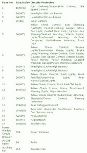
    Fuse Box BMW 733i 1982 Diagram And Power Distribution Fuse Box Map

    Fuse Box BMW 733i 1982 Diagram And Power Distribution Fuse Box Map - Here are new post for Fuse Box BMW 733i 1982 Diagram And Power Distribution Fuse Box Map.

    Fuse Box BMW 733i 1982 Diagram And Power Distribution Fuse Box Map


    Fuse
    Fuse

    Glove Box Light; Heated Door Lock; Ignition Key Warning/Seatbelt Warning; Interior Lights; Lights:Turn/Hazard Warning; On-Boar Computer; Radio/Power Antenna; Active Check Control; Dash Lights; Front Park/Tail/Underhood Light; Rear Marker/LicenseLights; Active Check Control; Backup Lights/Transmission Range Lights; Brake Lining Warning; Cruise Control; Dash Lights; Gauges; Idle Speed Control; Interior Lights; Power Mirrors; Power Windows; Trunk Light, Fuel Delivery/Evaporative Control; Idle Speed Control, Headlights , Cigar Lighters, Active Check Control; Auto Charging Flashlight; Central Locking; Gauges; Radio/Power Antenna; Stoplights/Cruise Control; Warning Indicators, Rear Defogger/Sunroof, Automatic Heater-Air Conditioner; Auxiliary Fan; Vacuum pump, FOglights(RH), Seatbelt Warning; Speedometer; Warning Indicators, Headlights,
    Read More..

    Monday, September 8, 2014

    Build a Power Supply Variable 1 3V 12 2V 1A Wiring diagram Schematic

    Build a Power Supply Variable 1.3V - 12.2V 1A Circuit Diagram. In this schema R2 to set the output voltage. The maximum current is determined by R3, over-current protection schema inside the LM723 to detect the voltage on R3, if it reaches 0.65 V, the voltage output will be off her. So the current through R3 can not exceed 0.65 / R3 although output short-schema in his.

    Power Supply Variable 1.3V - 12.2V 1A Circuit Diagram

    Power


    C3 and C4 are ceramic capacitors, as much as possible directly soldered to the PCB, this is because the LM723 is prone to oscillation that is not cool.

    LM723 works with 9.5V input voltage to 40 V DC and the LM723 can generate its own current of 150mA when the output voltage is not more than 6-7V under input voltage.

    Specifications:

    Output (value estimated):

    Vmin = (R4 + R5) / (R5 * 1.3)

    Vmax = (7.15 / R5) * (R4 + R5)

    Imax = 0.65/R3

    Max. Power on R3: 0.42/R3

    Min. DC Input Voltage (pin 12 to pin 7): Vmax + 5

    Parts List:

    B1 40V/2.5A

    C1 2200uF (3300uF even better)

    C2 4.7uF

    C3 100nF

    C4 1NF

    C5 330nF

    C6 100uF

    Green LED D1

    D2 1N4003

    F1 0.2A F

    F2 2A M

    IC1 LM723 (in a DIL14 plastic package)

    R1 1k

    R2 Pot. 5k

    R3 0.56R/2W

    R4 3.3k

    R5 4.7k

    S1 250V/1A

    T1 2N3055 on a heatsink 5K / W

    TR1 220V/17V/1.5 
    Read More..

    Low Power Wireless Audio Power Amplifier

    Battery-Powered portable unit, Suitable for all type Televisions

    Using this low-cost project one can reproduce audio from TV without disturbing others. It does not use any wire connection between TV and Loud Speaker. In place of a pair of wires, it uses invisible infra-red light to transmit audio signals from TV to Loud speakers, Without using any lens a range of up to 6 meters is possible. Range can be extended by using lenses and reflectors with IR sensors comprising transmitters and receivers.

    Transmitters operation:

    IR transmitter uses two-stage transistor amplifier to drive two series-connected IR LEDs. An audio output transformer (T1) is used (in reverse) to couple audio output from TV to the IR transmitter. Transistors Q1 and Q2 amplify the audio signals received from TV through the audio transformer. Low impedance output windings (lower gauge or thicker wires) are used for connection to TV side while high-impedance windings are connected to IR transmitter. This IR transmitter can be powered from a 9V mains adapter or a 9V battery. Red LED (D1) in transmitter schema functions as a Zener diode (0.65V) as well as supply-on indicator.

    Transmitter diagram:
     wireless audio power amplifier transmitter schematic schema diagram
    Wireless Audio Power Amplifier Transmitter Circuit Diagram

    Receivers operation:
    IR receiver uses popular op-amp IC µA741 and audio-frequency amplifier IC LM386 along with phototransistor L14F1 (Q3) and some discrete components. The sound generated by TV set is transmitted through IR LEDs, received by phototransistor Q3 and fed to pin 2 of IC µA741 (IC1). Its gain can be varied using potmeter P2. The output of IC µA741 is fed to IC LM386 (IC2) via capacitor (C7) and potmeter P3. The sound produced is heard through the receiver’s loudspeaker. Potmeter P3 is used to control the volume of loudspeaker SPKR (8-ohm, 1W).

    Receiver diagram:
     wireless audio power amplifier reciever schematic schema diagram
    Wireless Audio Power Amplifier Transmitter Circuit Diagram

    Parts:

    P1 = 10K
    P3 = 10K
    P2 = 1M

    R1 = 4.7K
    R2 = 22K
    R3 = 100R
    R4 = 10R-1W
    R5 = 10K
    R6 = 10K
    R7 = 15K
    R8 = 15K
    R9 = 100K
    R10 = 680R-1W
    R11 = 1K
    R12 = 10R-1W

    C1 = 220uF-25V
    C2 = 220uF-25V
    C3 = 10uF-25V
    C4 = 220uF-25V
    C5 = 220uF-25V
    C6 = 100nF-63V
    C7 = 100nF-63V
    C8 = 100nF-63V
    C9 = 100nF-63V

    D1 = Red LED
    D2 = IR LEDs
    D3 = IR LEDs

    Q1 = BC547
    Q2 = BD140
    Q3 = L14F1

    IC1 = uA741 Opamp
    IC2 = LM386

    J1 = Audio input Jack
    T1 = Audio Transformer
    SPKR = 1W-8ohm
    Read More..

    Sunday, September 7, 2014

    Memory Save on Power down Wiring diagram Schematic

    Memory Save on Power down Circuit Diagram. The auxiliary output powers the memory, while the main output powers the system and is connected to the memory store pin. When power goes down, the main output goes low, commanding the memory to store. The auxiliary output then drops out.

    Memory Save on Power down Circuit Diagram

    /
    Read More..