Friday, October 17, 2014
Simple Park Aid Circuit Diagram
Black surfaces lower greatly the device sensitivity. Obviously, you can use this circuit in other applications like liquids level detection, proximity devices etc. Circuit operation: IC1 forms an oscillator driving the infra-red LED by means of 0.8mSec. pulses at 120Hz frequency and about 300mA peak current. D1 & D2 are placed facing the car on the same line, a couple of centimeters apart, on a short breadboard strip fastened to the wall. D2 picks-up the infra-red beam generated by D1 and reflected by the surface placed in front of it. The signal is amplified by IC2A and peak detected by D4 & C4. Diode D3, with R5 & R6, compensates for the forward diode drop of D4. A DC voltage proportional to the distance of the reflecting object and D1 & D2 feeds the inverting inputs of three voltage comparators. These comparators switch on and off the LEDs, referring to voltages at their non-inverting inputs set by the voltage divider resistor chain R7-R10.

- Power supply must be regulated (hence the use of IC3) for precise reference voltages. The circuit can be fed by a commercial wall plug-in adapter, having a DC output voltage in the range 12-24V.
- Current drawing: LEDs off 40mA; all LEDs on 60mA @ 12V DC supply.
- The infra-red Photo Diode D2, should be of the type incorporating an optical sunlight filter: these components appear in black plastic cases. Some of them resemble TO92 transistors: in this case, please note that the sensitive surface is the curved, not the flat one.
- Avoid sun or artificial light hitting directly D1 & D2.
- If your car has black bumpers, you can line-up the infra-red diodes with the (mostly white) license or number plate.
- It is wiser to place all the circuitry near the infra-red LEDs in a small box. The 3 signaling LEDs can be placed far from the main box at an height making them well visible by the car driver.
- The best setup is obtained bringing D2 nearer to D1 (without a reflecting object) until D5 illuminates; then moving it a bit until D5 is clearly off. Usually D1-D2 optimum distance lies in the range 1.5-3 cm.
- If you are needing a simpler circuit of this kind driving a LED or a relay, click Infra-red Level Detectorv

Thursday, October 16, 2014
Simple Car Alarm Arming Horn Beep Canceller

| C1 | 1 | 0.01uF Ceramic Disc Capacitor | |
| C2 | 1 | 100uF 35V Electrolytic Capacitor | |
| R1 | 1 | 1K 1/4W Resistor | |
| R2 | 1 | 10K 1/4W Resistor | |
| R3 | 1 | 15K 1/4W Resistor | |
| R4 | 1 | 470 Ohm 1/4W Resistor | |
| D1, D3, D4 | 3 | 1N4004 Rectifier Diode | |
| D2 | 1 | Red LED | |
| U1 | 1 | 555 Timer IC | |
| K1 | 1 | SPST 12V Automotive Relay | |
| MISC | 1 | Board, Wire, Socket For U1, Case |
Simple 0 50V 2A Bench Power Supply Circuit Diagram

Vlose p1=100uA*Rp1
This lose voltage regulate output voltage rate of output current is compare between reference voltage of P3 and lose voltage on R11.T3 is protecting short circuit with R11. For reduce out put voltage to 0v should parallel one resistor 470 ohm in out put. Minimum voltage is 0.4v. The maximum output voltage is fixed with R1b and should not become over of 50v. Therefore your transformer should give 36V, 3A with 4700uF capacitor. T6, T5, T7 need heatsilk.
R1b = read the text
R2 = 10 K
R3, R7 = 3.3 k
R4 = 390 Ohm
R5 = 47 K
R6 = 3.3 K 1Watt
R8 = 180 Ohm
R9, R10 = 0.47 Ohm 3Watt
R11 = 0.075 Ohm 2Watt
R12 = 470 Ohm
P1 = 500K liner potentiometer
P2 = 4.7 K potentiometer
P3 = 10 K potentiometer
C1 = 1nF
C2 = 10nF
C3 = 22nF
C4 = 47mF 63v electrolytic
C5 = 4700mF 80v electrolytic
T1, T2 = BC161
T3, T4 = BD141
T5 = BD241
T6, T7 = 2V3055
D1, D2 = 1N4148
D3, D4 = 1N4001
IC1, IC2 = LM10C
Wednesday, October 15, 2014
Simple Frequency Voltage Converter Circuit Diagram

Wednesday, September 24, 2014
Simple Schmitt Trigger Circuits

One cheap IC, ul.914, can be used as an extremely simple and effective Schmitt trigger suitable for many applications. Hysterisis of the circuit is about 0.1 Volt. This may be varied by altering the values of R1 and R2.

An LED and phototransistor optical coupler system may be used to lengthen a three microsecond pulse to 55 milliseconds by using the values shown in the diagram. This allows complete isolation between input pulse circuits and the lengthener to be obtained.

Simple Baud Rate Generator Circuit IC 4060 Output Pin Out Configurations

Each serial data interface requires a baud rate generator: terminal, printer tape interface. . . lt is often not possible to use the same generator for input and output, so it would be useful to add one to, for instance, the UART in the computer or the UART in the terminal. To keep the ,costs of such an addition down, we have developed a generator which uses just one IC, two resistors, one preset potentiometer and a capacitor. The CMOS 4060 is a 14-stage binary counter with an internal oscillator which only requires the frequency determining RC components. As the reset is connected to earth, the counter begins to count upwards when the supply is switched on. A clock frequency then becomes available at the outputs: the higher the number of the output, the lower the frequency available at it.
In the circuit shown the frequencies avail- able at the various outputs are: O4 = 9600 baud 08 = 600 baud 05 = 4800 baud O9 = 300 baud O6 = 2400 baud Q10 = 150 baud Q7 = 1200 baud If the outputs are wired as shown in the circuit diagram, the required baud rate can then be selected by means of a wire link. _ The oscillator frequency can be set precisely with P1, and measured either at pin 9 of the 4060 or at one of the outputs O4 . . . Q10. With the values shown, the frequency at pin 9 should be 38.4 kl-lz; at the outputs O4. . .010 the relevant baud rate. lt is often required that the clock frequency is 16 times the baud rate (for instance, with asynchronous ~ operation of the 6850, 8251, 280- SIO. . .). ln that case, C1 must be replaced by a 27 nF capacitor and the oscillator frequency must be set to 614.4 kHz.
Friday, September 19, 2014
Simple 4 Channel Video Amplifier using NJM2582
A very simple 4 channel video amplifier electronic circuit project can be designed using NJM2582 ic suitable for video applications with SCART connector . Design of the circuit is very simple and require few external electronic parts .
Circuit diagram :

Simple 4 Channel Video Amplifier Circuit Diagram
Some features of the NJM2582 are : Operating Voltage ±5V, +5V, +11V ; 6input 4output , 2input 1output Video SW , Internal LPF , 6dB Amplifier , Internal 75Ω Driver Circuit , DC output for SCART (FUNCTION SW, BLANKING) .
Monday, September 8, 2014
Simple Tactful Triac Controller Wiring diagram Schematic
Simple Tactful Triac Controller Circuit Diagram
Sunday, September 7, 2014
Simple Light Dependent Resistors
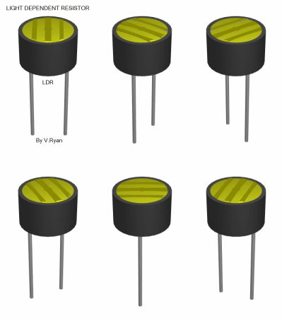
The animation opposite shows that when the torch is turned on, the resistance of the LDR falls, permitting current to have it.Circuit Wizard software has been used to show, the vary of values of a ORP12, LDR .
When a light-weight level of a thousand lux (bright light) is directed towards it, the resistance is 400R (ohms).

When a light-weight level of ten lux (very low light level) is directed towards it, the resistance has risen dramatically to ten.43M (10430000 ohms).
When the sunshine level is low the resistance of the LDR is high. This prevents current from flowing to the bottom of the transistors. Consequently the LED doesnt lightweight. However, when lightweight shines onto the LDR its resistance falls and current flows into the bottom of the primary transistor and then the second transistor. The LED lights.
The preset resistor will be turned up or right down to increase or decrease resistance, during this means it will build the schema additional or less sensitive. Link

Saturday, September 6, 2014
Simple Low Power Car Stereo Amplifier
A simple low power car stereo amplifier schema based on TDA 2003 is shown here. The schema uses cheap, readily available components and it is very easy to construct. TDA2003 is an integrated car radio amplifier from ST Micro electronics that has a lot of good features like short schema protection for all pins, thermal over range low harmonic distortion, low cross over distortion etc.
Circuit diagram :
A simple low power car stereo amplifier Circuit Diagram
In the schema given here each TDA2003 is wired as a mono amplifier operating from a 12V supply. Resistors R2 and R3 forms a feedback network that sets the amplifiers gain. C7 is the input DC de-coupling capacitor and C5 couples the speaker to the amplifiers output. C4 is used for improving the ripple rejection while C1 and C2 are employed for power supply filtering. C3 and R1 are used for setting the upper frequency cut-off. Network comprising of C6 and R4 is used for frequency stabilization and to prevent oscillation.
Notes.
- Assemble the schema on a good quality PCB.
- Heat sinks are necessary for both ICs.
- The schema can be operated from 12V DC.
- S1 is the ON/OFF switch
Friday, September 5, 2014
Simple 555 Tester Wiring diagram Schematic
Simple Meter Impedance speaker Wiring diagram Schematic
How to make the measurement of impedance speaker with the multimeter
Connect a digital multimeter to AC voltage in the range of 200mV.
Connect the device under test terminals
SW1 to R7, if the value of the measured impedance is less than 100 ohm R8 or upwards.
With SW2 in the "Set" power-on schema through SW3
Adjust P1 to read exactly 100.0mV the display DVM
Switch SW2 in the "Measure" and read directly from the speaker or headphones impedance value on the display DVM, eg 8.2mV = 8.2 Ohm / 80.1mV = 80.1 Ohm
How to make the measurement of impedance speaker with the oscilloscope:
Connect the oscilloscope instead of DVM (multimeter) and turn P1 fully clockwise.
Short the output speaker and adjust R3 to get a sine wave amplitude of about 2.2V peak-to-peak.
How to make the impedance measurement Speaker "By ear"
Connect a small speaker or headphones, forming a pair of headphones to the output of the schema and turn P1 to obtain a level of sound output moderated. Carefully adjust R3 until the output sound stops, then turn the trimpot to adjust slowly and stop immediately when the sound start again.
List of components
P1 4K7 linear potentiometer
R1 12K 1/4W Resistor
R2 2K2 1/4W Resistor
R3 1K 1/2W Trimmer (cermet)
R4 1K5 1/4W Resistor
4K7 1/4W Resistor R5
R6 3K3 1/4W Resistor
R7 100R 1/4W Resistor (See Notes)
R8 1K 1/4W Resistor (See Notes)
R9 1K 1/4W Resistor (Optional)
22NF 63V Polyester Capacitor C1
C2 330nF 63V Polyester Capacitor
C3 22μF 25V Electrolytic Capacitor
D1, D2 1N4148 75V 150mA Diodes
D3 3mm red LED (Optional)
Q1, Q2, Q3 BC550C 45V 100mA Low noise High gain NPN
IC1 78L05 5V 100mA Regulator IC
SW1, SW2 SPDT Toggle or Slider
SW3 SPST switch or Slider
B1 9V PP3 battery for PP3Clip
Notes:
For very precise measurements using resistors R7 and R8 with 1% or 2% tolerance.
D3 LED pilot and his current limiting resistor R9 are optional.
Thursday, September 4, 2014
Simple LCD Module in 4 bit Mode
The LCD module was driven directly by a microcontroller, which was on a development board for testing various programs and I/O functions. There was a switch present for turning off the enable of the display when it wasn’t being used, but this could be forgotten during some experiments. When the R/Wline of the display is permanently tied to GND (data only goes from the microcontroller to the display) then the remaining lines can safely be connected to the supply (+ve or GND). In this application however, the R/Wline was also controlled by the microcontroller. When the display is initialised correctly then nothing much should go wrong. The data sheet for the HD44780 is not very clear as to what happens with the low nibble during initialisation.

Copyright: Elektor Electronics
Wednesday, September 3, 2014
Simple Toss A Coin Binary Box Wiring diagram Schematic
Simple Toss A Coin Binary Box Circuit Diagram
Simple Knight Rider lights Circuit for model cars
Simple Knight Rider lights Circuit Diagram
Note
That VDD and GND for the ICs are not shown in the schema drawing.
| Pin-outs: | |||||
| (7)555 | 4017 | ||||
| 1 | GND | 1 | Q5 | 9 | Q8 |
| 2 | TRIGGER | 2 | Q1 | 10 | Q4 |
| 3 | OUTPUT | 3 | Q0 | 11 | Q9 |
| 4 | RESET | 4 | Q2 | 12 | CO |
| 5 | CONTROL VOLTAGE | 5 | Q6 | 13 | NOT ENABLE |
| 6 | THRESHOLD | 6 | Q7 | 14 | CLK |
| 7 | DISCHARGE | 7 | Q3 | 15 | RESET |
| 8 | VDD | 8 | GND | 16 | VDD |
Tuesday, September 2, 2014
Simple Circuit Board Checker
Simple Circuit Board Checker Circuit diagram

Parts:
R1 = 22K
R2 = 22K
D1 = Red LED
D2 = Green LED
Q1 = BF245
Q2 = BC547
Q3 = BC557
Notes:
- The Black clip must be connected to the negative ground of the board under test.
- The Red clip should be connected to a positive voltage source (not exceeding 30V) available on the same board.
- Metal probe is suitable for this schema.
- Two Miniature Crocodile Clips (Red and Black) are also necessary.
Monday, September 1, 2014
Simple Battery charger Wiring diagram Schematic

Saturday, August 30, 2014
LM317 Simple Audio Amplifier Circuits
| LM317 Simple Audio Amplifier Circuits |
